Hot-carrier injection programmable memory and method of programming such a memory

a programmable memory and hot-carrier technology, applied in solid-state devices, instruments, semiconductor devices, etc., can solve the problems of occupying more semiconductor surfaces of split-gate memory cells than conventional flash memory cells, and unable to control injection performance as efficiently

Active Publication Date: 2015-12-29
STMICROELECTRONICS INT NV
View PDF14 Cites 12 Cited by
  • Summary
  • Abstract
  • Description
  • Claims
  • Application Information

AI Technical Summary

Problems solved by technology

Offsetting their good injection performance, split gate memory cells have the disadvantage of occupying more semiconductor surface than conventional flash memory cells, that are also programmed by hot-electron injection but comprise only one control gate.
Moreover, providing a single gate forming both a control gate and a selection gate does not enable the injection performance to be controlled as efficiently as with a conventional split gate memory cell of the type represented in FIG. 1.

Method used


Image

  • Hot-carrier injection programmable memory and method of programming such a memory
  • Hot-carrier injection programmable memory and method of programming such a memory
  • Hot-carrier injection programmable memory and method of programming such a memory

Examples


first embodiment

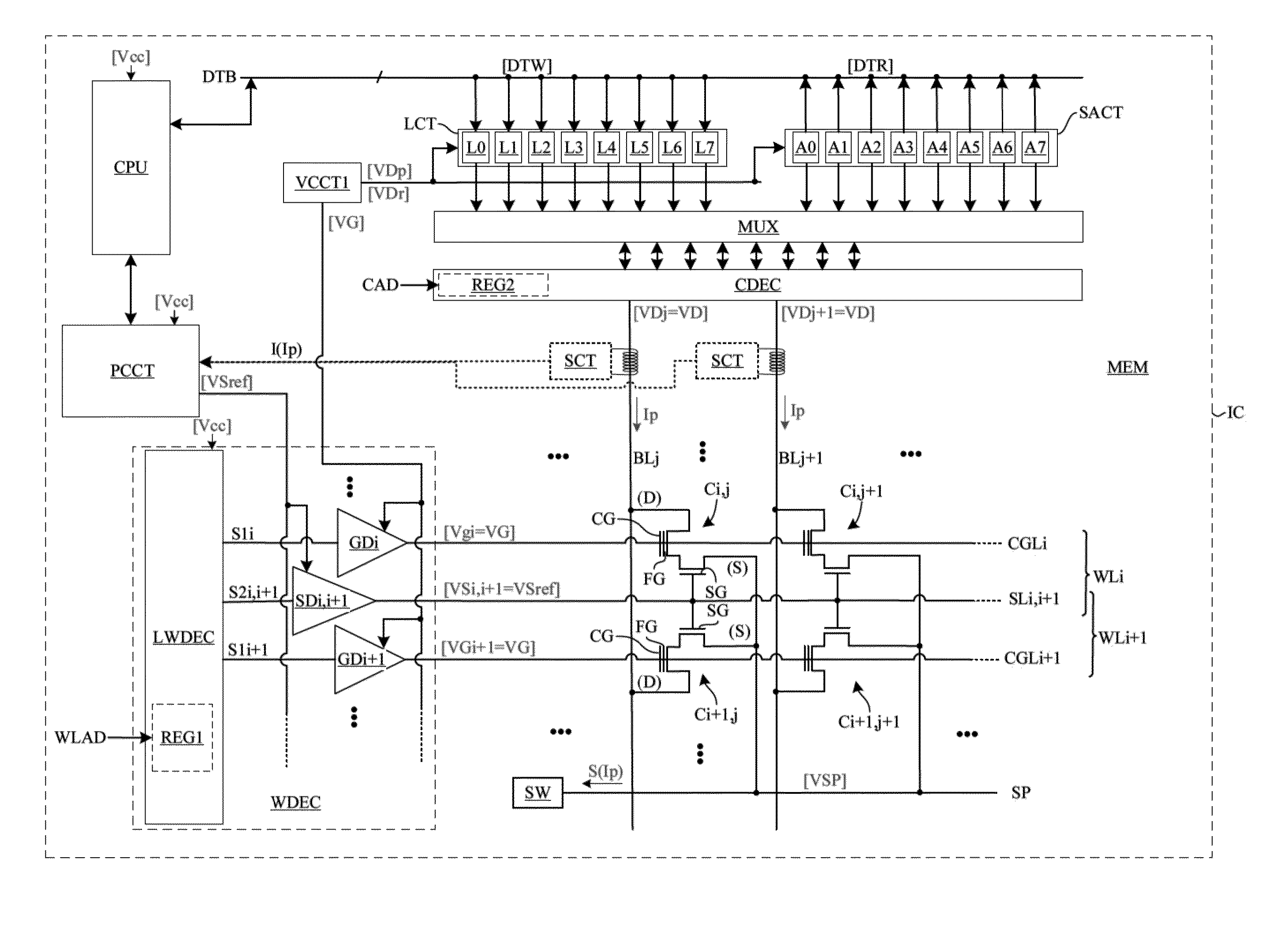
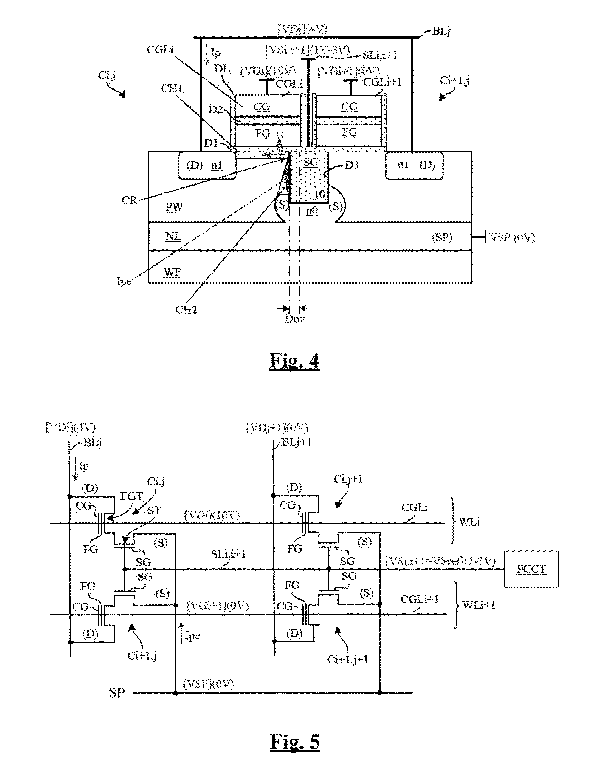
[0069]FIG. 7 shows one embodiment PCCT1 of the circuit PCCT implementing the method, using here the voltage / current response from a test memory cell. The circuit PCCT1 here comprises two test memory cells EC1, EC2, a circuit VCCT2 supplying DC voltages Vpass and Vc, a current generator IG2, and a comparator CP produced for example with an operational amplifier. The memory cells EC1, EC2 are twin memory cells the structure of which is identical to functional twin memory cells of the memory array, and are manufactured at the same time as the functional memory cells, preferably near the memory array or in a dedicated zone of the memory array. They only differ from the functional memory cells by the fact that they have an additional electrical contact enabling their floating gate FG to be electrically accessed. The drain D of each test memory cell EC1, EC2 is linked to a terminal N1 of the voltage source IG2 the other terminal of which receives a bias voltage VP. The terminal N1 is also...

second embodiment

[0089]FIGS. 8A and 8B show one embodiment PCCT2 of the circuit PCCT implementing the programming method according to the present disclosure. In this example of implementation of the method, the sense amplifiers of the memory A0-A7 are used as means for measuring the current circulating in the bit lines, to determine the selection voltage VSref enabling the targeted programming current Ipref to be obtained. For this purpose, the sense amplifiers used are of the type configurable by means of a register CREG connected to the data bus DTB, in which the unit CPU loads a read current threshold setpoint beyond which the output of the sense amplifiers A0-A7 changes its logic state.

[0090]This mode of executing the method avoids providing current sensors in each bit line. Indeed, a sense amplifier is after all nothing more than a binary current sensor supplying a bit having a first logical value, for example 0, when the current passing through the memory cell being read is below a current thr...


PUM


Abstract

The present disclosure relates to a memory comprising at least one word line comprising a row of split gate memory cells each comprising a selection transistor section comprising a selection gate and a floating-gate transistor section comprising a floating gate and a control gate. According to the present disclosure, the memory comprises a source plane common to the memory cells of the word line, to collect programming currents passing through memory cells during their programming, and the selection transistor sections of the memory cells are connected to the source plane. A programming current control circuit is configured to control the programming current passing through the memory cells by acting on a selection voltage applied to a selection line.

Description

BACKGROUND[0001]1. Technical Field[0002]The present disclosure relates to integrated circuit memories comprising split gate memory cells, each comprising a selection transistor section and a floating-gate transistor section. The selection transistor section comprises a selection gate and the floating-gate transistor section comprises a floating gate and a control gate.[0003]2. Description of the Related Art[0004]So-called “split gate” memory cells are conventionally programmed by hot-electron injection (or “hot-carrier injection”). Compared to tunnel-effect programming, programming by hot electrons has the advantage of being short, generally 100 times shorter than tunnel-effect programming. For a better understanding, the programming time of a memory cell by hot-electron injection is typically in the order of a few microseconds compared to a few milliseconds for tunnel-effect programming.[0005]During hot-electron programming, the two transistor sections of the memory cell cooperate ...

Claims


Application Information

Patent Timeline
Patent Type & Authority Patents(United States)
IPC IPC(8): G11C16/00H01L29/423G11C16/34G11C16/04H01L29/788H01L27/115G11C16/10
CPCG11C16/10G11C16/0425G11C16/0433H01L29/7881H01L27/11524H01L29/42328H01L29/42336G11C16/34G11C16/08G11C16/24G11C16/3418H10B41/35
Inventor LA ROSA, FRANCESCONIEL, STEPHANREGNIER, ARNAUDDELALLEAU, JULIEN
Owner STMICROELECTRONICS INT NV
Why Eureka
Try Eureka