Methods for promoting semiconductor manufacturing yield and classifying defects during fabricating a semiconductor device, and computer readable mediums encoded with a computer program implementing the same

a technology of semiconductor manufacturing and defect classification, applied in the field of semiconductor manufacturing, can solve the problems of reducing so as to reduce the manufacturing cycle time, reduce the number of defects, and define the hotspot area more accurately

Active Publication Date: 2016-02-02
ASML NETHERLANDS BV
View PDF8 Cites 13 Cited by
  • Summary
  • Abstract
  • Description
  • Claims
  • Application Information

AI Technical Summary

Benefits of technology

[0017]In contrast to the conventional method for inspecting defects in a semiconductor device, the present invention can consider effect of each defect of the current layer to other layers, and effects of every defect to the current layer and / or other layers can be entirely figured out before the semiconductor device is manufactured, so as to reduce manufacturing cycle times. In addition, each defect may be classified into DOI or unimportant defect or more precisely by using the present invention, so as to define hotspot areas more accurately and further reduce manufacturing cycle times by neglecting the unimportant defects during manufacturing the semiconductor device. Accordingly, the present invention can increase or promote total yield of manufacturing the semiconductor device.

Problems solved by technology

However, the above-mentioned inspecting method can only define effect of each defect to the current inspected layer, but effect of each defect to other layers or even to the whole device cannot be taken into consideration.
In addition, each defect may be classified according to its effect to the current layer only, not the whole device, so that the classification and the hot spots defined according to the classification are limited.
Thus, only inspecting on patterns of the current layer may misjudge hot spot area, and lower classification precision.

Method used


Image

  • Methods for promoting semiconductor manufacturing yield and classifying defects during fabricating a semiconductor device, and computer readable mediums encoded with a computer program implementing the same
  • Methods for promoting semiconductor manufacturing yield and classifying defects during fabricating a semiconductor device, and computer readable mediums encoded with a computer program implementing the same
  • Methods for promoting semiconductor manufacturing yield and classifying defects during fabricating a semiconductor device, and computer readable mediums encoded with a computer program implementing the same

Examples


Embodiment Construction

[0025]Reference will now be made in detail to specific embodiments of the present invention. Examples of these embodiments are illustrated in the accompanying drawings. While the invention will be described in conjunction with these specific embodiments, it will be understood that it is not intended to limit the invention to these embodiments. In fact, it is intended to cover alternatives, modifications, and equivalents as may be included within the spirit and scope of the invention as defined by the appended claims. In the following description, numerous specific details are set forth in order to provide a through understanding of the present invention. The present invention may be practiced without some or all of these specific details. In other instances, well-known process operations are not described in detail in order not to obscure the present invention.

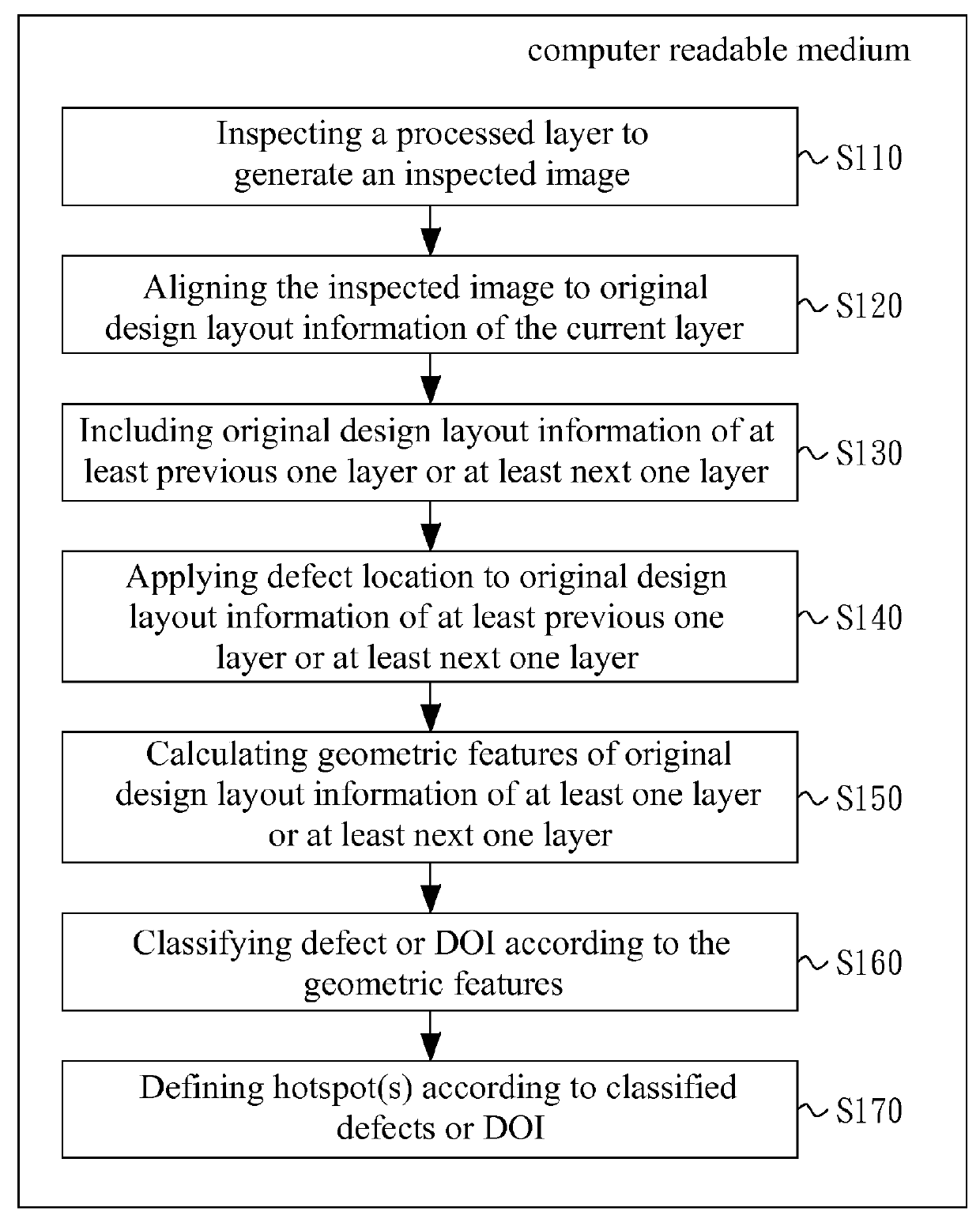
[0026]FIG. 1 illustrates a block diagram of a method for promoting semiconductor manufacturing yield according to an embodim...


PUM

PropertyMeasurementUnit
semiconductor manufacturing yieldaaaaaaaaaa
scanning electron microscopeaaaaaaaaaa
semiconductoraaaaaaaaaa

Abstract

A method for promoting semiconductor manufacturing yield comprising the following steps and a computer readable medium encoded with a computer program implementing the method is provided. First, a processed layer is inspected to generate an inspected image with defects thereon. Next, the inspected image is aligned to an original design layout information of the processed layer. In addition, the defects are classified according to geometric features of the original design layout information of the processed layer and at least previous one layer and/or at least next one layer.

Description

FIELD OF THE INVENTION[0001]The present invention generally relates to semiconductor manufacturing, and more particularly to a method for classifying defects to promote semiconductor manufacturing yield.DESCRIPTION OF THE RELATED ART[0002]How to inspect defects in a semiconductor device is one of the major subjects in a semiconductor fabricating process. A conventional method for inspecting defects is using a scanning electron microscope (SEM) system to scan the semiconductor device layer by layer during a fabrication process of the semiconductor device, so as to capture scanned images, such as SEM images, of all layers, and then the presence of defects at each layer may be determined by inspecting the scanned images.[0003]For example, the SEM system may be used to scan a patterned semiconductor layer after the patterned semiconductor layer is formed on a substrate, and thus the presence of defects at the patterned semiconductor layer may be determined by inspecting the scanned imag...

Claims


Application Information

Patent Timeline
Patent Type & Authority Patents(United States)
IPC IPC(8): G06T7/00G01N21/95
CPCG06T7/001G01N21/9501G06T2207/30148G03F7/7065H01L22/12H01L22/20
Inventor CHEN, SHIH-TSUNGFANG, WEIFU, YU-TSORNGPENG, FUTANGZHANG, ZHAO-LI
Owner ASML NETHERLANDS BV
Why Eureka
Try Eureka