Methods of producing strain in a semiconductor waveguide and related devices

a technology of semiconductor waveguides and strainers, applied in the direction of optical waveguide light guides, instruments, optics, etc., can solve the problems of only occurrence of shg effect, difficult integration and manufacture, and most materials are not optically transparent, so as to reduce or eliminate strain in sections, the effect of high strain

Active Publication Date: 2016-02-16
NAT TECH & ENG SOLUTIONS OF SANDIA LLC
View PDF4 Cites 9 Cited by
  • Summary
  • Abstract
  • Description
  • Claims
  • Application Information

AI Technical Summary

Benefits of technology

[0008]Embodiments of invention described herein eliminate the need to reverse or “flip” the sign of an optical mode coupling coefficient, X2. This is made possible because the inventors recognized that silicon and germanium do not naturally exhibit a X2 effect. Therefore, second order optical effects can be achieved by applying a high strain only to alternating sections of a waveguide that have a high X2 while reducing or eliminating strain in sections that do not have a high X2.

Problems solved by technology

Most materials are not optically transparent in these regions or are difficult to integrate and manufacture.
First, the SHG effect only occurs at wavelengths of 2 μm to 1 μm that have no significant commercial applications.
Second, the efficiency of the conversion is poor, due to the lack of phase matching methods which results in coherent and constructive build up of power from a pump wavelength (e.g., 2 μm) to a generated output optical wavelength (e.g., 1 μm).
However, the structures described by Hon appear to be difficult to manufacture, and do not appear to offer long wave infrared transparency.
Still further, Hon's alternating strains appear to apply high stresses on silicon structures, which can lead to defects or even failure of the crystal structure (e.g., cracking).

Method used


Image

  • Methods of producing strain in a semiconductor waveguide and related devices
  • Methods of producing strain in a semiconductor waveguide and related devices
  • Methods of producing strain in a semiconductor waveguide and related devices

Examples


Embodiment Construction

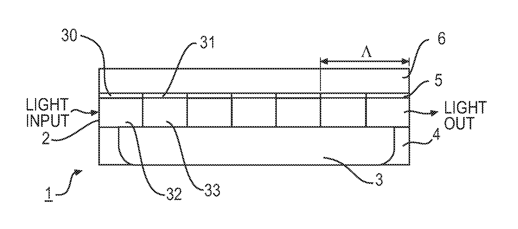
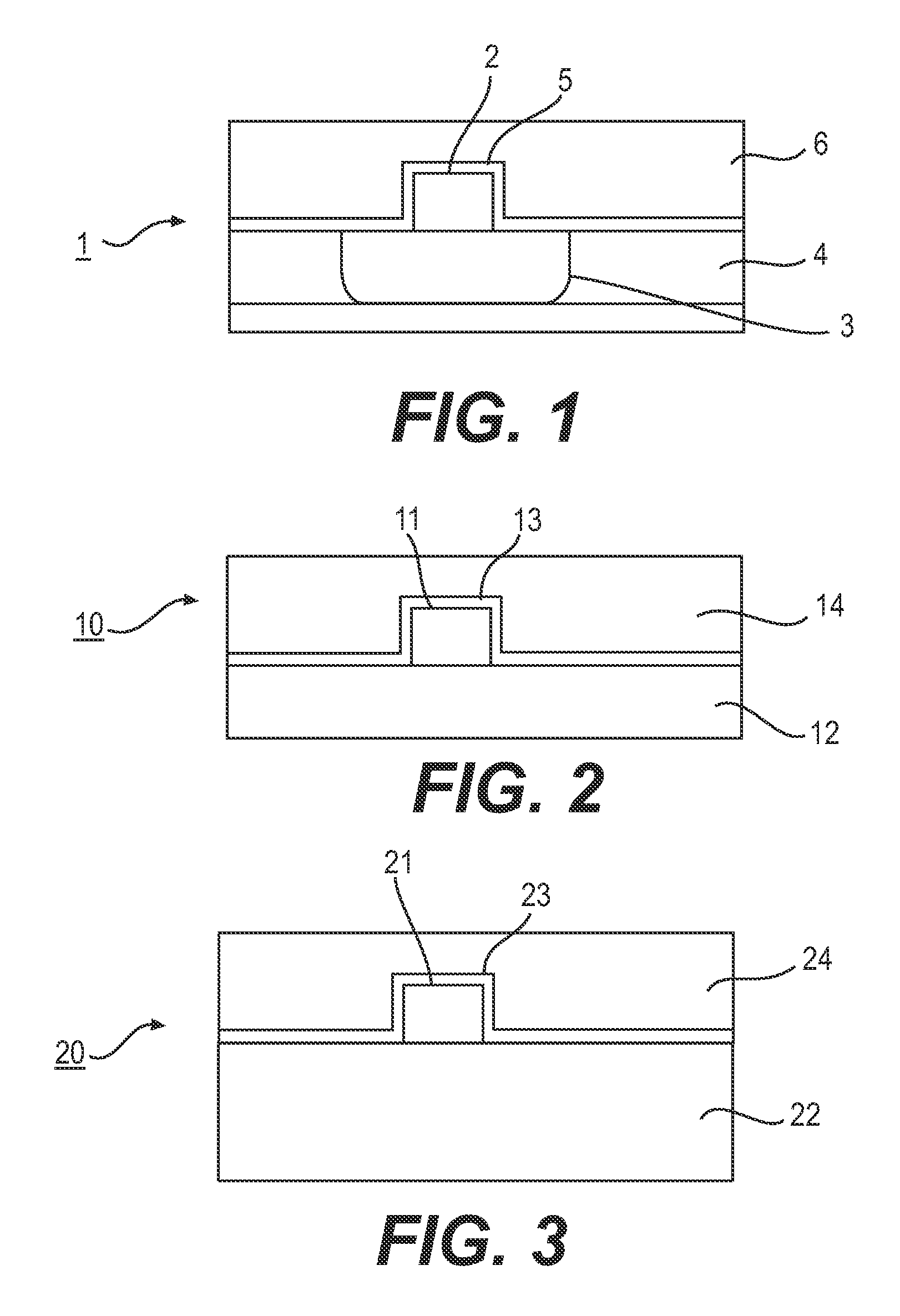
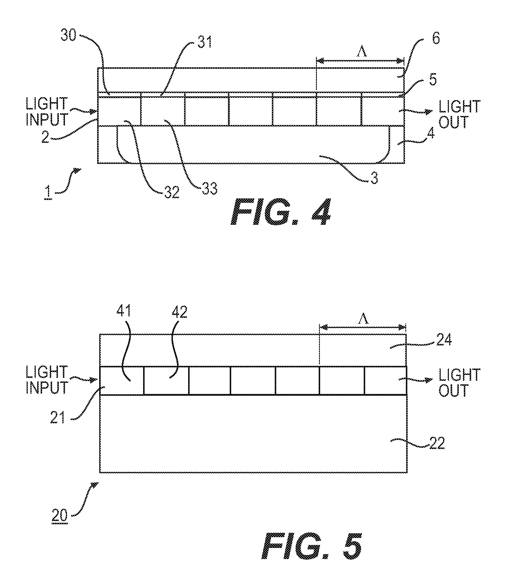
[0033]Throughout the following description and drawings, like reference numbers / characters refer to like elements. It should be understood that, although specific exemplary embodiments are discussed herein there is no intent to limit the scope of present invention to such embodiments. To the contrary, it should be understood that the exemplary embodiments discussed herein are for illustrative purposes, and that modified and alternative embodiments may be implemented without departing from the scope of the present invention.

[0034]It should be further noted that some exemplary embodiments may be described and claimed as a process or method (hereafter “method”). Though a method may be described and claimed as set of sequential steps, it should be understood that the steps may be performed in parallel, concurrently or simultaneously. In addition, the order of each step within a method may be re-arranged. A method may be terminated when completed, and may also include additional steps no...


PUM


Abstract

Quasi-phase matched (QPM), semiconductor photonic waveguides include periodically-poled alternating first and second sections. The first sections exhibit a high degree of optical coupling (abbreviated “X2”), while the second sections have a low X2. The alternating first and second sections may comprise high-strain and low-strain sections made of different material states (such as crystalline and amorphous material states) that exhibit high and low X2 properties when formed on a particular substrate, and/or strained corrugated sections of different widths. The QPM semiconductor waveguides may be implemented as silicon-on-insulator (SOI), or germanium-on-silicon structures compatible with standard CMOS processes, or as silicon-on-sapphire (SOS) structures.

Description

GOVERNMENT LICENSE RIGHTS[0001]This invention was developed under Contract DE-AC04-94AL85000 between Sandia Corporation and the U.S. Department of Energy. The U.S. Government has certain rights in this invention.INTRODUCTION[0002]It has previously been proposed to use common crystalline semiconductor materials as photonic waveguides in the near infrared. For example, Soref, “Mid-Infrared Photonics in Silicon and Germanium,” Nature Photonics, vol. 4, pp. 495-497 (August 2010), points out that silicon and germanium are potentially ideal for the generation and manipulation of light on chips in medium wavelength infrared (MWIR) to long wavelength infrared (LWIR) applications (e.g., 3-12 μm), because silicon and germanium are optically transparent in these regions. Most materials are not optically transparent in these regions or are difficult to integrate and manufacture.[0003]In addition, it has previously been proposed to use induced-strain to achieve second order harmonic generation (...

Claims


Application Information

Patent Timeline
Patent Type & Authority Patents(United States)
IPC IPC(8): G02B6/12G02B6/10
CPCG02B6/12G02B6/12014G02B6/12011G02B6/12009G02B6/122G02F1/3558
Inventor COX, JOHATHAN ALBERTRAKICH, PETER THOMAS
Owner NAT TECH & ENG SOLUTIONS OF SANDIA LLC
Why Eureka
Try Eureka