
Manufacturing method of a flexible display

a manufacturing method and flexible technology, applied in the field of display, can solve the problems of reducing the yield rate, affecting the quality of the product, and the tool cannot be easily inserted into the middle of the glass substrate and the plastic substrate, so as to achieve the effect of preventing the damage to the plastic substrate in the separation process, facilitating the finishing process, and facilitating the production

Active Publication Date: 2016-03-15
TCL CHINA STAR OPTOELECTRONICS TECH CO LTD
View PDF3 Cites 2 Cited by
  • Summary
  • Abstract
  • Description
  • Claims
  • Application Information

AI Technical Summary

Benefits of technology

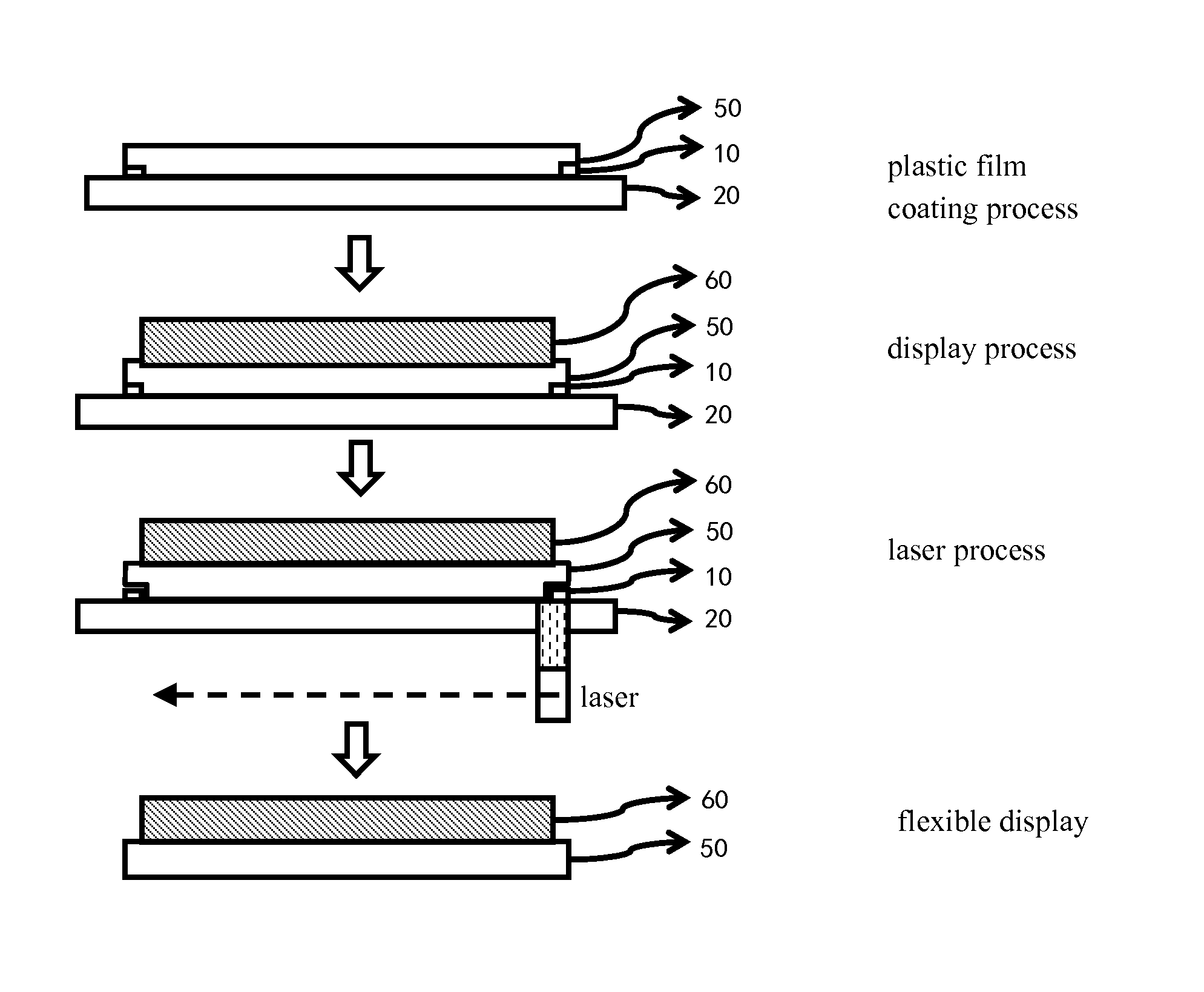
The present invention provides a manufacturing method for a flexible display that solves issues in the prior art. Specifically, the method includes steps to separate the plastic substrate from the glass substrate without causing damage or low yield rate. To achieve this, a frame-type amorphous silicon layer containing hydrogen is added between the substrates to improve the separation process. After coating the plastic substrate and producing the display, a laser is used to dehydrogenate the substrates and generate hydrogen gas to separate the edges of the substrates. This simplifies the separation process and prevents damage to the plastic substrate. The technical effect of this method is to improve the manufacturing of flexible displays and increase production yield.

Problems solved by technology

However, there is a flaw in the process of removing the plastic substrate, since the bonding of the plastic substrate to the glass substrate is too high, tools can not be easily inserted into the middle of the glass substrate and the plastic substrate.
Therefore, the difficulty in the separation of the plastic substrate and the glass substrate is prone to cause damage to the plastic film and lower the yield rate.

Method used


Image

  • Manufacturing method of a flexible display
  • Manufacturing method of a flexible display
  • Manufacturing method of a flexible display

Examples


Embodiment Construction

[0021]For making the object of the present invention, technical solutions, and beneficial effects more clearly understood, the embodiments in the present invention in conjunction with the accompanying drawings will be described below in detail. It should be understood that the specific embodiments described herein are merely to illustrate the invention, and are not used to limit the present invention.

[0022]In the present embodiment of the present invention, before a plastic substrate and a glass undergo an attachment process, a process is added to form frame-type amorphous silicon containing hydrogen in a high concentration. After a display film, such as LCD, EPD or OLED display film, is finished, a laser is used in a dehydrogenating process, and hydrogen gas can be generated by the dehydrogenation. The hydrogen gas generated can separate the peripheral edges of the plastic substrate from the glass substrate, so that the subsequent separation process of a plastic substrate and the g...


PUM

PropertyMeasurementUnit
yield rateaaaaaaaaaa
flexibleaaaaaaaaaa
flexibilityaaaaaaaaaa

Abstract

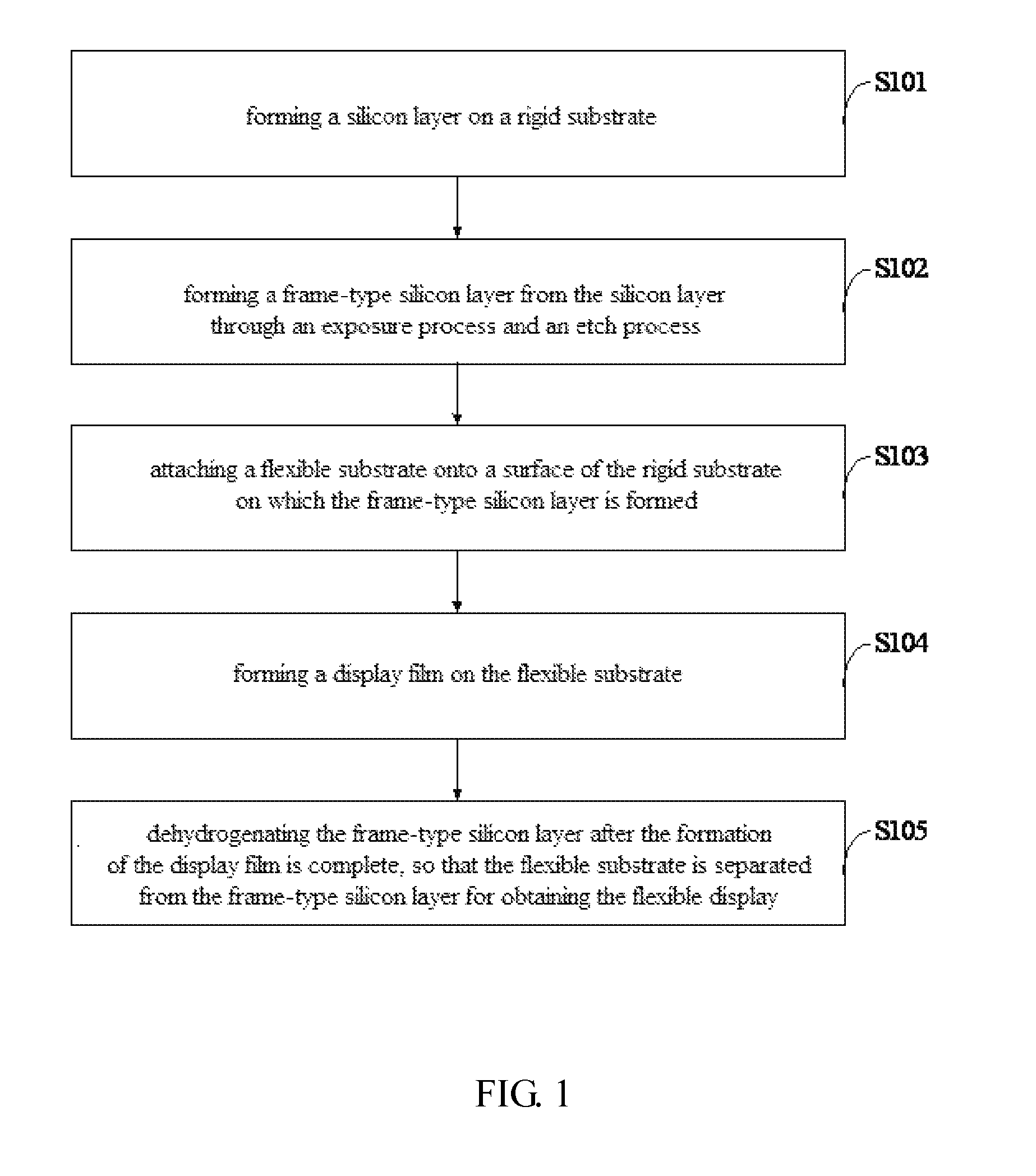
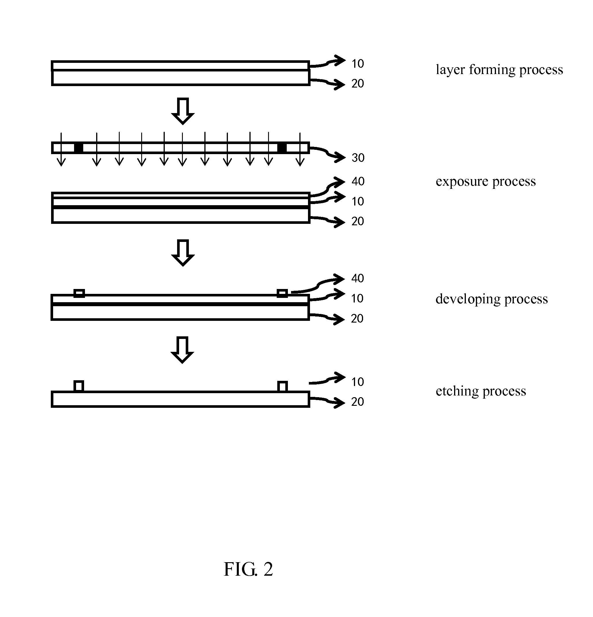
A manufacturing method of a flexible display is provided, which comprises steps of forming an silicon layer on a rigid substrate, forming a frame-type silicon layer from the silicon layer, attaching a flexible substrate onto the surface of the rigid substrate on which the frame-type amorphous silicon layer is formed, forming a display film on the flexible substrate, and dehydrogenating the frame-type silicon layer after the formation of the display film is complete, so that the flexible substrate is separated from the frame-type silicon layer for obtaining the flexible display. The manufacturing method of the flexible display prevents the problem of low yield rate caused by the damage to the plastic substrate in the separation process.

Description

FIELD OF THE INVENTION [0001]The present invention relates to the display field, in particular a manufacturing method of a flexible display.BACKGROUND OF THE INVENTION[0002]Currently, flexible displays are the trend of the next generation of displays. The advantages thereof are flexibility, lightweight and easy to carry, and can be used in the wearable device.[0003]The existing flexible display manufacture process is attaching a plastic substrate onto a glass substrate, waiting until after the producing process of the LCD (Liquid Crystal Display), EPD (Electro-Phoretic Display) or OLED (Organic Light-Emitting Diode), etc, and then removing the plastic substrate from the glass substrate.[0004]However, there is a flaw in the process of removing the plastic substrate, since the bonding of the plastic substrate to the glass substrate is too high, tools can not be easily inserted into the middle of the glass substrate and the plastic substrate. Therefore, the difficulty in the separation...

Claims


Application Information

Patent Timeline
Patent Type & Authority Patents(United States)
IPC IPC(8): H01J9/00H01J9/20
CPCH01J9/20H01L27/1266H01L21/6835H01L2221/68318H01L2221/6835H01L2221/68381G02F1/133305
Inventor SU, CHANG-ICHENG, YANGLING
Owner TCL CHINA STAR OPTOELECTRONICS TECH CO LTD
Learn More