Semiconductor device and method for manufacturing the same

a semiconductor device and semiconductor technology, applied in the direction of semiconductor devices, electrical appliances, transistors, etc., can solve the problems of increasing the amount of change in electrical characteristics of transistors, poor electrical characteristics, etc., to improve the reliability of a semiconductor device or the like reduce the defect of an oxide semiconductor film of a semiconductor device including an oxide semiconductor film, and improve the electrical characteristics of a semiconductor device.

Active Publication Date: 2016-03-15
SEMICON ENERGY LAB CO LTD
View PDF143 Cites 27 Cited by
  • Summary
  • Abstract
  • Description
  • Claims
  • Application Information

AI Technical Summary

Benefits of technology

[0010]Thus, an object of one embodiment of the present invention is to reduce defects in an oxide semiconductor film of a semiconductor device including the oxide semiconductor film. Another object of one embodiment of the present invention is to improve electrical characteristics of a semiconductor device including an oxide semiconductor film. Another object of one embodiment of the present invention is to improve reliability of a semiconductor device including an oxide semiconductor film.
[0017]In accordance with one embodiment of the present invention, defects in an oxide semiconductor film of a semiconductor device including the oxide semiconductor film can be reduced. Further, in accordance with one embodiment of the present invention, the electrical characteristics of a semiconductor device including an oxide semiconductor film can be improved. Further, in accordance with one embodiment of the present invention, reliability of a semiconductor device or the like including an oxide semiconductor film can be improved.

Problems solved by technology

In a transistor using an oxide semiconductor film, there are a large number of oxygen vacancies in the oxide semiconductor film, which causes poor electrical characteristics of the transistor and causes an increase in the amount of change in electrical characteristics of the transistor, typically the threshold voltage due to a change over time or a stress test (e.g., a bias-temperature (BT) stress test).

Method used


Image

  • Semiconductor device and method for manufacturing the same
  • Semiconductor device and method for manufacturing the same
  • Semiconductor device and method for manufacturing the same

Examples


embodiment 1

(Embodiment 1)

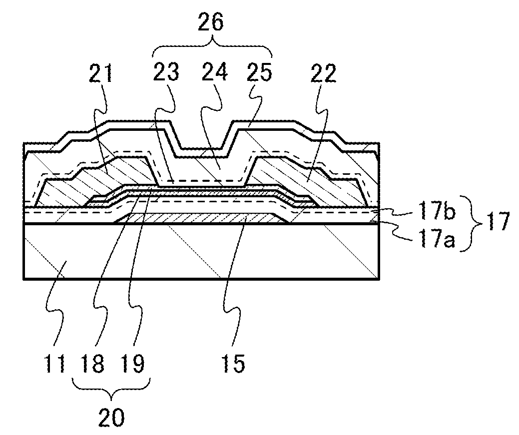
[0058]In this embodiment, a semiconductor device which is one embodiment of the present invention and a manufacturing method thereof are described with reference to drawings.

[0059]In a transistor including an oxide semiconductor film, oxygen vacancies are given as an example of a defect which leads to poor electrical characteristics of the transistor. For example, the threshold voltage of a transistor including an oxide semiconductor film which contains oxygen vacancies in the film easily shifts in the negative direction, and such a transistor tends to have normally-on characteristics. This is because electric charges are generated owing to oxygen vacancies in the oxide semiconductor film and the resistance is thus reduced. The transistor having normally-on characteristics causes various problems in that malfunction is likely to be caused when in operation and that power consumption is increased when not in operation, for example. Further, there is a problem in that th...

embodiment 2

(Embodiment 2)

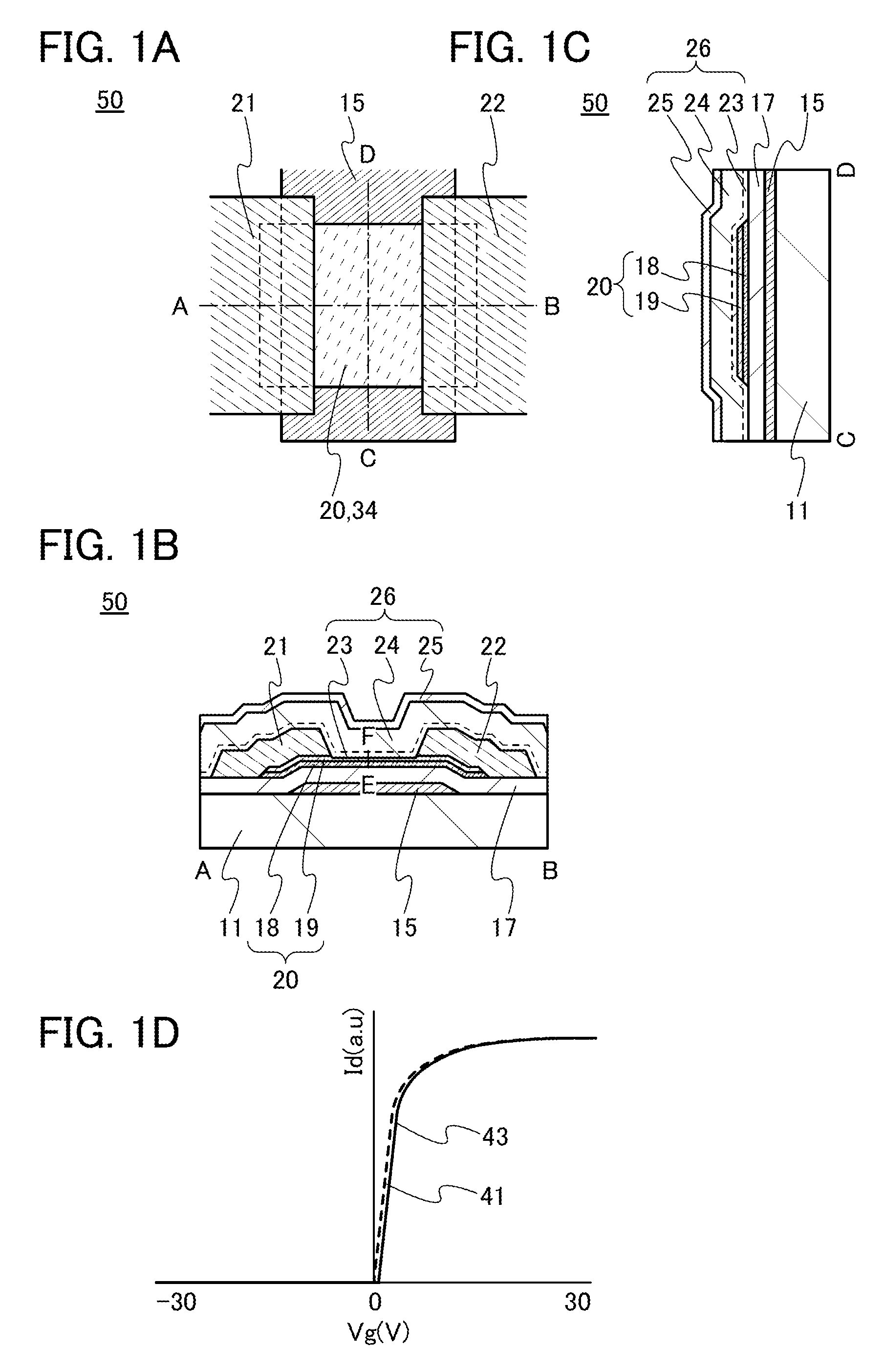
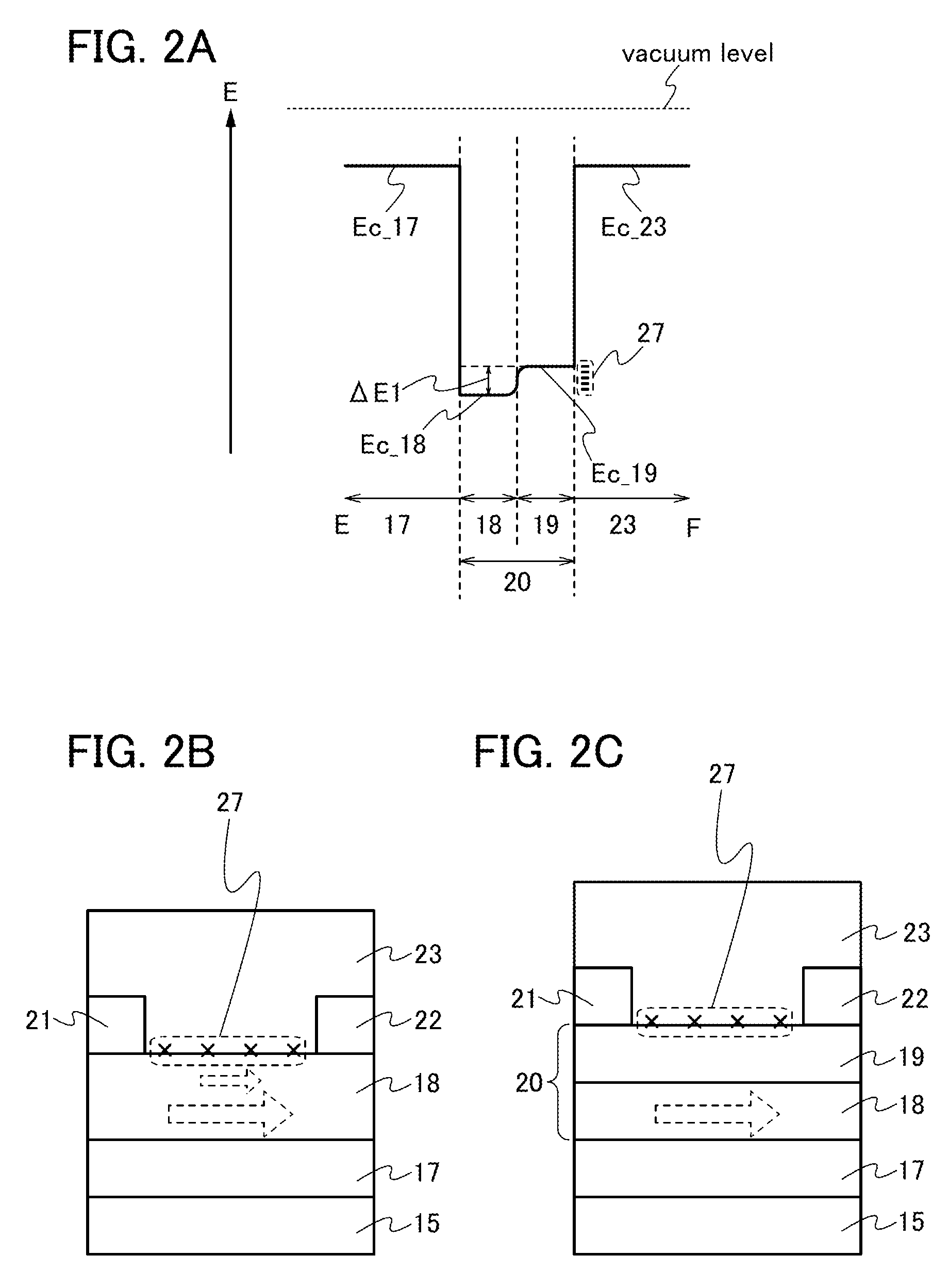
[0202]In this embodiment, a semiconductor device having a transistor in which the number of defects in the oxide semiconductor film can be further reduced as compared to Embodiment 1 is described with reference to drawings. The transistor described in this embodiment is different from that in Embodiment 1 in having an oxide film containing In or Ga between the gate insulating film and the oxide semiconductor film.

[0203]FIGS. 6A to 6E are a top view and cross-sectional views of a transistor 60 included in the semiconductor device. FIG. 6A is a top view of the transistor 60, FIG. 6B is a cross-sectional view taken along dashed-dotted line A-B of FIG. 6A, and FIG. 6C is a cross-sectional view taken along dashed-dotted line C-D of FIG. 6A. Note that in FIG. 6A, the substrate 11, the gate insulating film 17, the oxide insulating film 23, the oxide insulating film 24, the nitride insulating film 25, and the like are omitted for simplicity.

[0204]The transistor 60 shown in FIG...

embodiment 3

(Embodiment 3)

[0264]In this embodiment, a transistor having a different structure from the transistors in Embodiment 1 and Embodiment 2 is described with reference to FIG. 13. A transistor 70 described in this embodiment includes a plurality of gate electrodes facing each other with an oxide semiconductor film provided therebetween.

[0265]The transistor 70 shown in FIG. 13 includes the gate electrode 15 provided over the substrate 11. Further, the gate insulating film 17 is formed over the substrate 11 and the gate electrode 15, and the multilayer film 20 overlapping with the gate electrode 15 with the gate insulating film 17 provided therebetween, and the pair of electrodes 21 and 22 in contact with the multilayer film 20 are included. Note that the multilayer film 20 includes the oxide semiconductor film 18 and the oxide film 19 containing In or Ga. Furthermore, the protective film 26 including the oxide insulating film 23, the oxide insulating film 24, and the nitride insulating f...


PUM


Abstract

In a semiconductor device including a transistor including a gate electrode formed over a substrate, a gate insulating film covering the gate electrode, a multilayer film overlapping with the gate electrode with the gate insulating film provided therebetween, and a pair of electrodes in contact with the multilayer film, a first oxide insulating film covering the transistor, and a second oxide insulating film formed over the first oxide insulating film, the multilayer film includes an oxide semiconductor film and an oxide film containing In or Ga, the oxide semiconductor film has an amorphous structure or a microcrystalline structure, the first oxide insulating film is an oxide insulating film through which oxygen is permeated, and the second oxide insulating film is an oxide insulating film containing more oxygen than that in the stoichiometric composition.

Description

BACKGROUND OF THE INVENTION[0001]1. Field of the Invention[0002]The present invention relates to a semiconductor device including a transistor and a method for manufacturing the semiconductor device.[0003]2. Description of the Related Art[0004]Transistors used for most flat panel displays typified by a liquid crystal display device and a light-emitting display device are formed using silicon semiconductors such as amorphous silicon, single crystal silicon, and polycrystalline silicon provided over glass substrates. Further, transistors formed using such silicon semiconductors are used in integrated circuits (ICs) and the like.[0005]In recent years, attention has been drawn to a technique in which, instead of a silicon semiconductor, a metal oxide exhibiting semiconductor characteristics is used for transistors. Note that in this specification, a metal oxide exhibiting semiconductor characteristics is referred to as an oxide semiconductor.[0006]For example, a technique is disclosed i...

Claims


Application Information

Patent Timeline
Patent Type & Authority Patents(United States)
IPC IPC(8): H01L21/00H01L29/786H01L21/02H01L29/51H01L29/66
CPCH01L29/78693H01L21/022H01L21/02263H01L29/513H01L29/66969H01L29/7869H01L29/78696H01L21/0262H01L21/02554H01L21/02565H01L29/24H01L29/78648
Inventor KOEZUKA, JUNICHISHIMA, YUKINORITOKUNAGA, HAJIMESASAKI, TOSHINARIMURAYAMA, KEISUKEMATSUBAYASHI, DAISUKE
Owner SEMICON ENERGY LAB CO LTD
Why Eureka
Try Eureka