Low clock-power integrated clock gating cell
a low clock-power, integrated technology, applied in the direction of power consumption reduction, logic circuits, pulse techniques, etc., can solve the problem of increasing power consumption
- Summary
- Abstract
- Description
- Claims
- Application Information
AI Technical Summary
Benefits of technology
Problems solved by technology
Method used
Image
Examples
Embodiment Construction
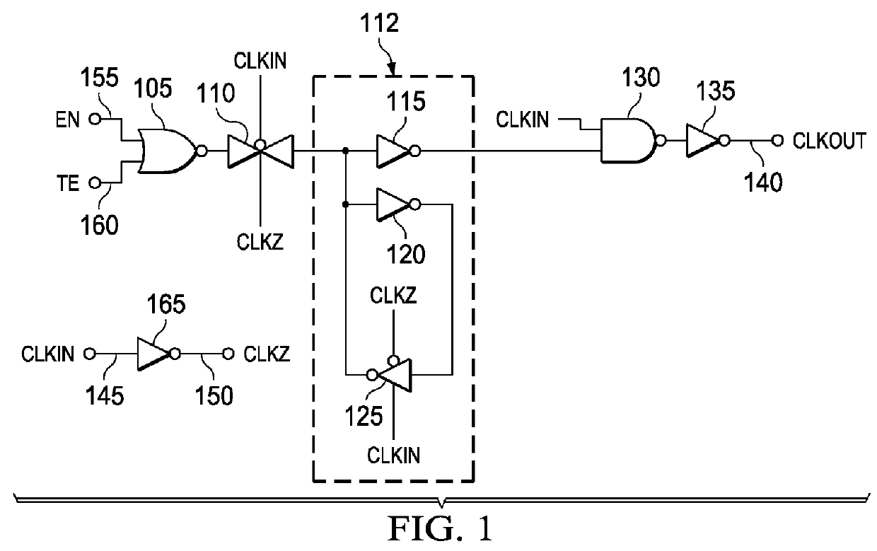
[0014]FIG. 1 illustrates a schematic of an ICG. The ICG includes a NOR gate 105 that receives a test enable signal 160 and an enable signal 155. The NOR gate 105 is coupled to a transmission gate 110. The transmission gate 110 receives a clock input CLKIN 145 and an inverted clock signal CLKZ 150. The inverted clock signal 150 is generated through an inverter 165 that receives the CLKIN 145 and outputs the inverted clock signal CLKZ 150. The output of the transmission gate is coupled to a latch 112 that includes an inverter 115 and back-to-back inverters 120 and 125. The inverter 125 is a tri-state inverter. Output of the latch 112 is coupled to a NAND gate 130. The clock input CLKIN 145 is also given as another input to the NAND gate 130. An output of the NAND gate 130 is coupled to an inverter 135 which generates the clock output CLKOUT on a line 140.
[0015]The operation of the ICG of FIG. 1 is explained now. Consider an example when the enable signal 155 is at logic 1 and the test...
PUM
 Abstract
Description
Claims
Application Information


