Plasma etching process

a technology of etching process and plasma, which is applied in the direction of basic electric elements, semiconductor/solid-state device manufacturing, electric devices, etc., can solve the problem of the intrinsic etching precision which can be obtained from plasma, the gate electrodes of fdsoi transistors are particularly delicate, and the etching b>120/b> of fdsoi transistors can be etched with precision. improve the effect of accuracy control of the reactive layer thickness and

Active Publication Date: 2016-06-28
COMMISSARIAT A LENERGIE ATOMIQUE ET AUX ENERGIES ALTERNATIVES +1
View PDF2 Cites 8 Cited by
  • Summary
  • Abstract
  • Description
  • Claims
  • Application Information

AI Technical Summary

Benefits of technology

[0031]The initial phase thus makes it possible to quickly etch the layer to be etched and the subsequent phase of etching is triggered when the thickness of the layer to be etched is reduced and when the free face of the layer to be etched gets close to the underlying layer. The subsequent phase is started soon enough for the underlying layer not to be affected. If the underlying layer is made of single-crystal silicon, the single-crystal silicon underlying layer will not be undesirably be etched.
[0082]The system thus makes it possible to form a pulsed reactive gas plasma in the reactor alternately with inert gas plasma. The injection device thus makes it possible to inject a first gas or a first mixture of gas into the plasma reactor, and then to interrupt such injection after a very short time, beyond which a second gas or a second mixture of gas is injected for an also very short time. The system is so configured as to be able to repeat this sequence as many times as required.

Problems solved by technology

However, plasma etching must be able to take up always more difficult challenges to face the introduction of new families or technological “nodes”, specifically beyond the so-called “22 nm” nodes.
Executing patterns of the order of ten nanometers (nm) then raises the problem of the intrinsic etching precision which can be obtained from plasma.
The main difficulty relates to the selectivity of etching at the boundary between the layers of different materials which the devices to be produced are made of.
Plasma-etching 120 the gate electrodes of the FDSOI transistors is particularly delicate.
In this case, a problem arises, specifically upon etching the gate, on the one hand 290 and the spacers on the other hand.
The risk of damaging the FIN top is real.
The problem arising during the production of such three-dimensional structure consists in not damaging the rectangular geometrical shape, and more particularly the corners 280 of the FIN, at the risk of severely affecting the performances of such type of transistors, the electric characteristics and behaviour of which are directly dependent on the shapes of the channel and of the surrounding gate 290.
Such a technique, which is essentially implemented in laboratories for developing new products is intrinsically long.
This method is so long that it is not industrialized.
The other disadvantage is that the directionality of low energy ions is not as important.
Etching is not as anisotropic as it used to be with high energy ions and complying with the critical dimensions (CD) of transistors with a decananometric size thus becomes difficult.
Etching with a low electronic temperature plasma is therefore not considered as a solution industrially viable at such integration level.
In such conditions, the energy transmitted to the ions is lower than when plasma is continuously operated, but the etching speed also becomes very low and does not meet the industrial expectations.

Method used


Image

  • Plasma etching process
  • Plasma etching process
  • Plasma etching process

Examples


Embodiment Construction

[0096]It should be noted that, within the scope of the present invention, the words “on”, “over” or “underlying” or the equivalents thereof do not necessarily mean “in contact with”. Thus, for instance, depositing a first layer on a second layer does not necessarily mean that the two layers are directly in contact with each other, but this means that the first layer at least partially covers the second layer by being either directly in contact therewith or by being separated therefrom by another layer or another element.

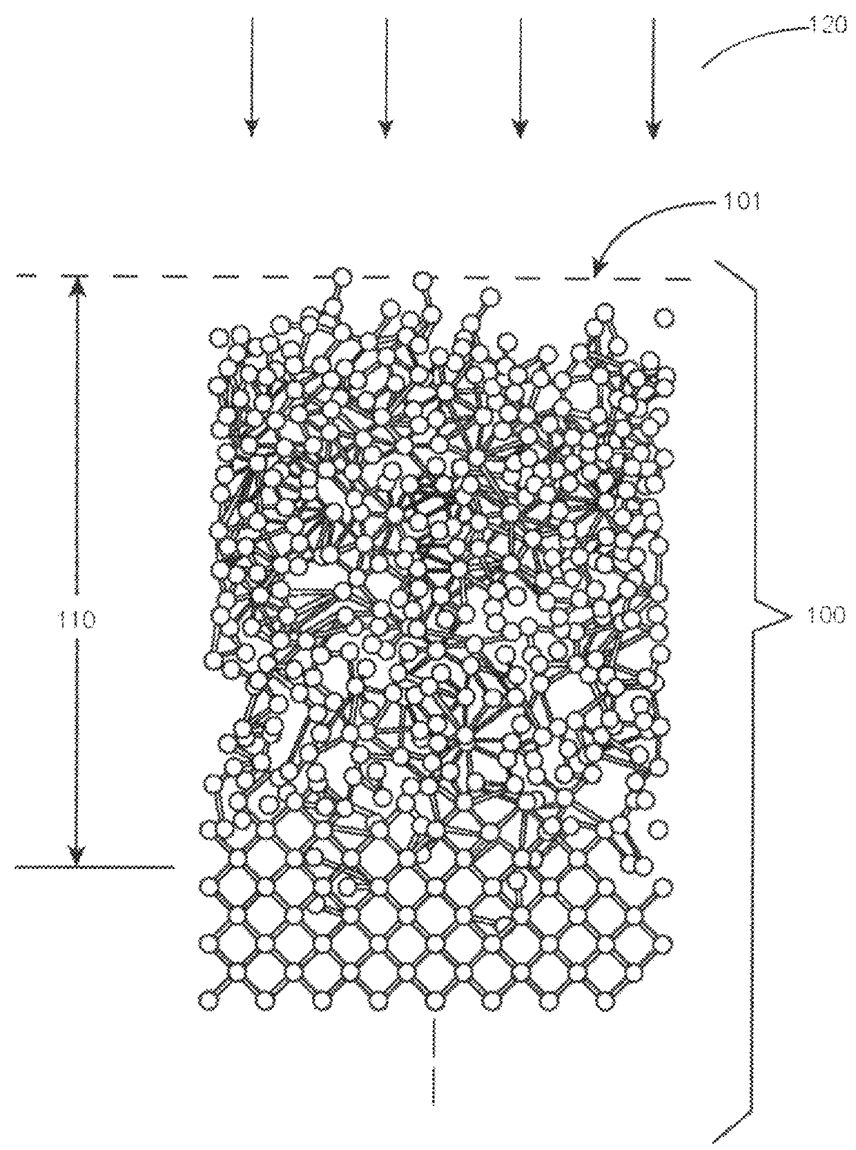
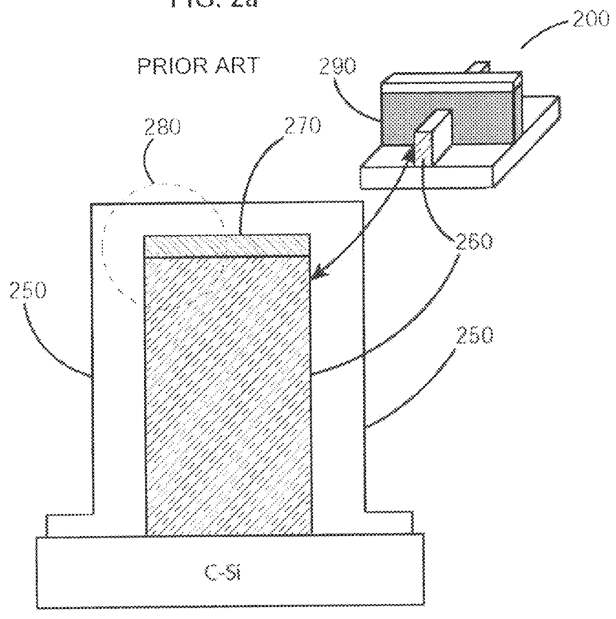
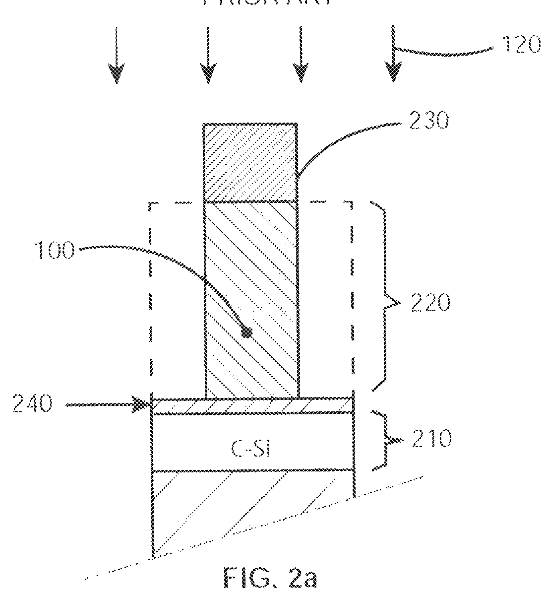
[0097]In the following description, thickness is generally measured in directions perpendicular to the plane of the lower face of the layer to be etched or of a substrate whereon the lower layer has been deposited. Thickness is thus generally measured along a vertical direction in the figures shown. On the contrary, the thickness of a layer covering a flank of a pattern is measured along a direction perpendicular to such flank.

[0098]The invention will now be describe...


PUM


Abstract

A method and system are provided for etching a layer to be etched in a plasma etching reactor, including: forming a reactive layer by injection of at least one reactive gas to form a reactive gas plasma, which forms, together with the layer to be etched, a reactive layer which goes into the layer to be etched during etching of said layer to be etched, wherein the reactive layer reaches a steady state thickness upon completion of a determined duration of said injection; said injection being interrupted before said determined duration has elapsed so that, upon completion of the forming of the reactive layer, the thickness of the reactive layer is smaller than said steady state thickness; and removing the reactive layer by injection of at least one inert gas to form an inert gas plasma, which makes it possible to remove only the reactive layer.

Description

TECHNICAL FIELD OF THE INVENTION[0001]The present invention generally relates to dry etching techniques used in microelectronics and more particularly concerns the improvement of accuracy in this type of etching using plasma.STATE OF THE ART[0002]The constant reduction in the dimensions of the patterns required to be etched to produce always denser integrated circuits could be sustained only by constantly improving the techniques of photolithography and etching of the layers of materials used to produce the electronic integrated circuits and all sorts of other devices of micrometric or nanometric sizes combining optical and mechanical devices.[0003]After having long used so-called “wet etching” wherein the substrates to be etched are immersed into an appropriate solution, capable of chemically reacting with the material to be etched and to dissolve it, the microelectronics industry has used so-called “dry etching” for many years. Such etching is obtained by ionic bombardment of the ...

Claims


Application Information

Patent Timeline
Patent Type & Authority Patents(United States)
IPC IPC(8): H01L21/302H01L21/3065H01L21/311H01L21/67
CPCH01L21/3065H01L21/31116H01L21/67069
Inventor JOUBERT, OLIVIERCUNGE, GILLESDESPIAU-PUJO, EMILIEPARGON, ERWINEPOSSEME, NICOLAS
Owner COMMISSARIAT A LENERGIE ATOMIQUE ET AUX ENERGIES ALTERNATIVES
Why Eureka
Try Eureka