System for verifying timing constraints of IC design

a timing constraint and timing constraint technology, applied in the field of electronic design automation tools, can solve the problems of increasing the time required for verifying the timing constraint of the integrated circuit design, reducing the yield of the ics, and increasing the complexity of the ics

Active Publication Date: 2016-09-20
NXP USA INC
View PDF3 Cites 4 Cited by
  • Summary
  • Abstract
  • Description
  • Claims
  • Application Information

AI Technical Summary

Problems solved by technology

This has led to an increase in the complexity of the ICs, thereby leading to a decrease in the yield of the ICs.
If data regarding the non-critical signal paths is not provided to the EDA tool for performing a static timing analysis (STA) of the netlist, the EDA tool analyzes the non-critical paths, which increases the time required for verifying the IC design.
As timing constraints in the timing constraint file are provided by the IC designer, some of the timing constraints may not be valid.
Thus, a critical signal path propagating the signal may not be verified correctly...

Method used


Image

  • System for verifying timing constraints of IC design
  • System for verifying timing constraints of IC design
  • System for verifying timing constraints of IC design

Examples


Embodiment Construction

[0022]The detailed description of the appended drawings is intended as a description of the currently preferred embodiments of the present invention, and is not intended to represent the only form in which the present invention may be practiced. It is to be understood that the same or equivalent functions may be accomplished by different embodiments that are intended to be encompassed within the spirit and scope of the present invention. As used herein, the term multiplexer has been abbreviated as a mux and the term de-multiplexer has been abbreviated as a demux.

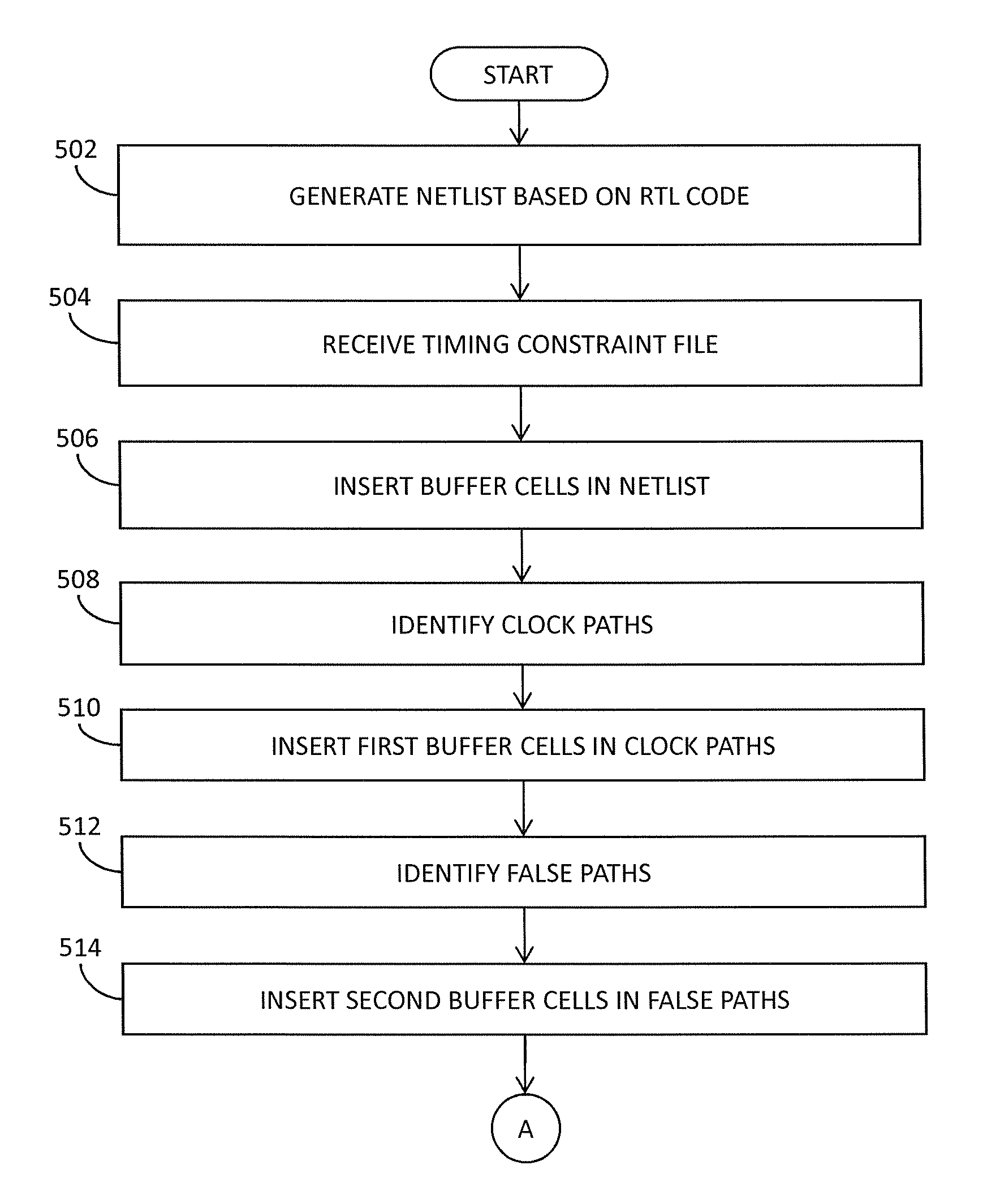
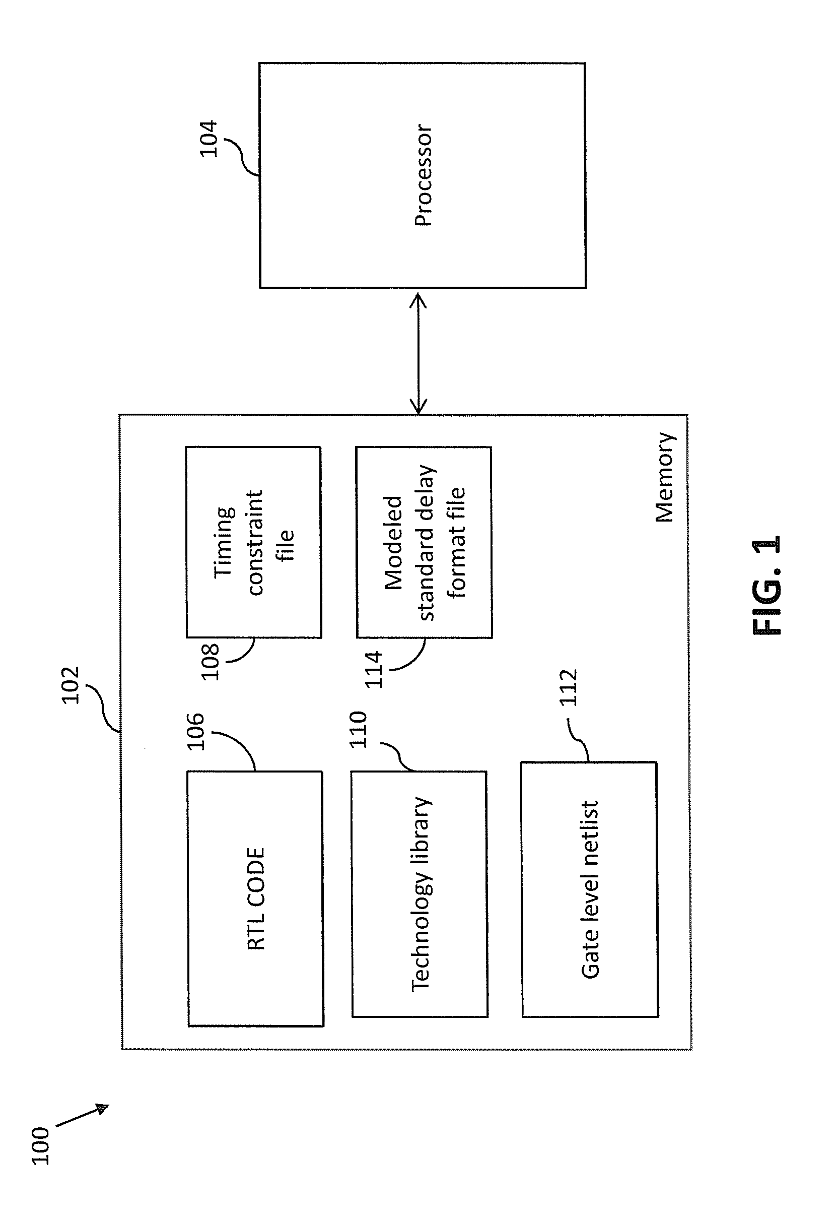
[0023]In an embodiment of the present invention, an electronic design automation (EDA) tool for verifying timing constraints of a netlist that is indicative of an integrated circuit (IC) design is provided. The EDA tool includes a memory and a processor in communication with the memory. The memory stores a register transfer level (RTL) code of the IC design and a timing constraint file. The timing constraint file includes as...


PUM


Abstract

An EDA tool for verifying timing constraints of an integrated circuit (IC) design includes a processor and a memory that stores register transfer level (RTL) code of the IC design and a timing constraint file. The processor generates a netlist based on the RTL code, and identifies asynchronous clock paths, false paths and multi-cycle paths in the netlist using the timing constraint file. The processor then inserts buffer cells for logic cells in the netlist. The processor also inserts buffer cells in the asynchronous clock paths, false paths, and multi-cycle paths. The processor delay annotates logic cells and clock delay cells with a zero delay value and the buffer cells with known delay values. The processor generates a modeled standard delay format (SDF) file and performs a gate level simulation (GLS) using the modeled SDF file.

Description

BACKGROUND OF THE INVENTION[0001]The present invention generally relates to electronic design automation (EDA) tools, and more particularly to an EDA tool for verifying timing constraints of an integrated circuit (IC) design.[0002]Integrated circuits (ICs) including system-on-chips (SoCs) integrate various digital and sometimes analog elements on a single chip. With advancements in semiconductor technology, the operational speed of ICs is increasing and more and more functions are being added to the ICs by increasing the number of circuit elements. This has led to an increase in the complexity of the ICs, thereby leading to a decrease in the yield of the ICs. Thus, testing and verifying a design during the design stage has become increasingly important.[0003]Testing and verification are performed by an EDA tool. In the front-end design stage, the operation of the IC design is described using a hardware description language (HDL) such as Verilog and very high speed integrated circuit...

Claims


Application Information

Patent Timeline
IPC IPC(8): G06F9/45G06F17/50
CPCG06F17/5031G06F17/5081G06F17/505G06F2111/04G06F30/3312
Inventor MISHRA, ATEETBELWAL, SHIVAMAHAJAN, DEEPAK
Owner NXP USA INC
Why Eureka
Try Eureka