Static random access memory

Active Publication Date: 2016-11-01
POWERCHIP SEMICON MFG CORP
View PDF5 Cites 2 Cited by
  • Summary
  • Abstract
  • Description
  • Claims
  • Application Information

AI Technical Summary

Benefits of technology

[0007]The invention provides a static random access memor

Problems solved by technology

However, memory cells of the conventional SRAM take up a relatively greater area, making it unable to effectively increase the

Method used


Image

  • Static random access memory
  • Static random access memory
  • Static random access memory

Examples


first embodiment

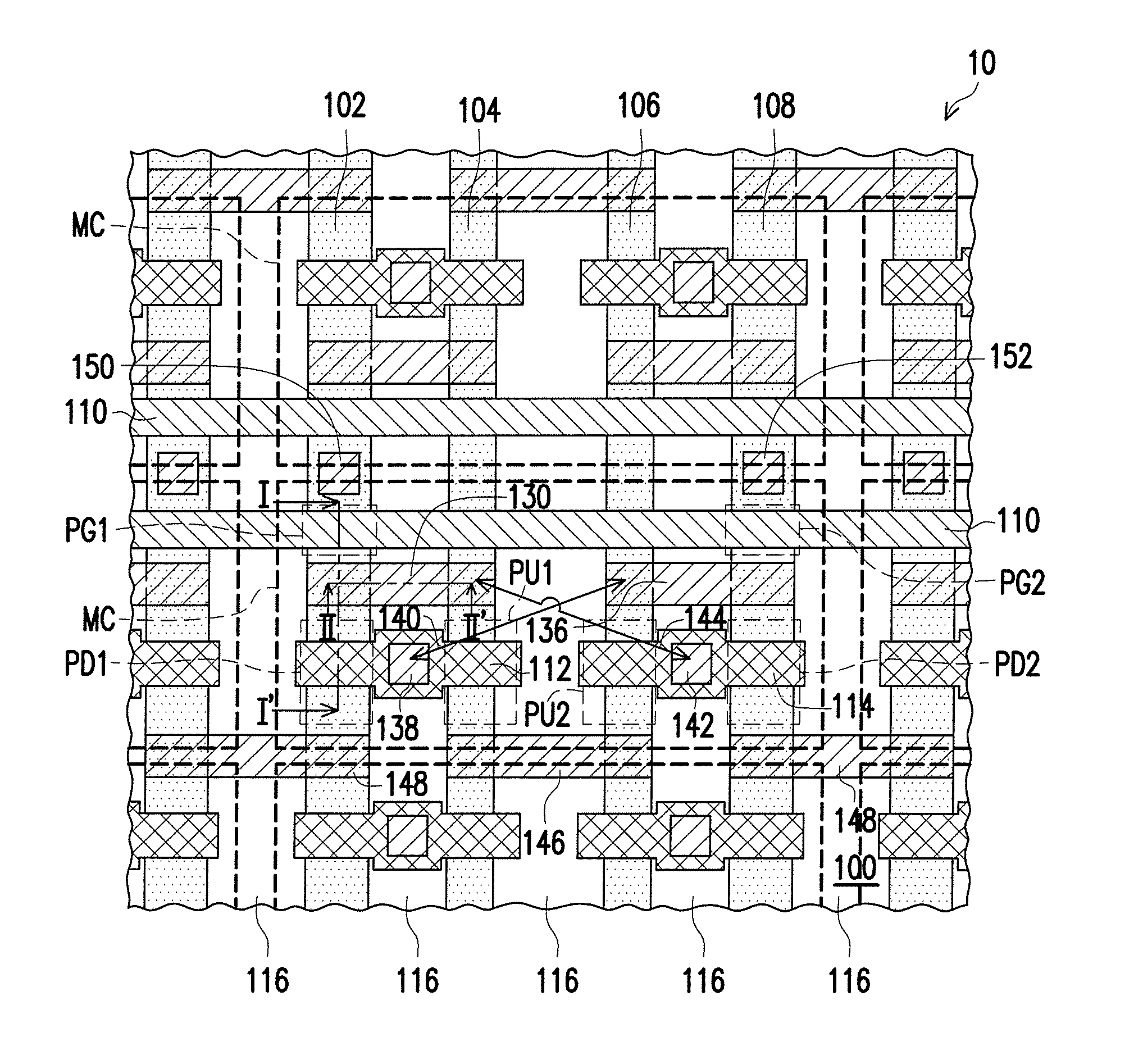
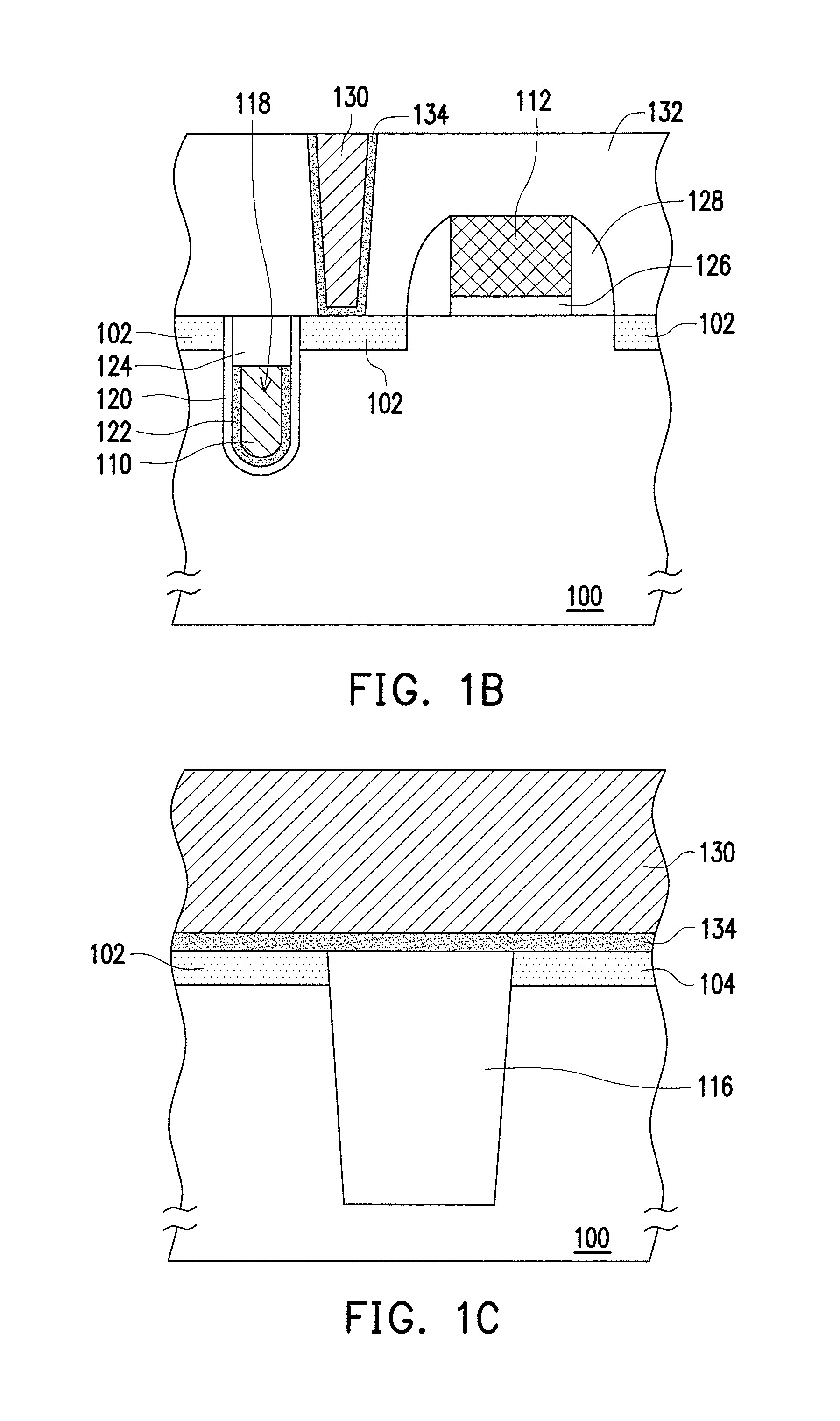
[0033]FIG. 1A is a top view illustrating a static random access memory according to the invention. In FIG. 1A, dielectric layers and spacers are omitted to make the description clearer. FIG. 1B is a cross-sectional view taken along a cross-sectional line I-I′ of FIG. 1A. FIG. 1C is a cross-sectional view taken along a cross-sectional line II-IP of FIG. 1A.

[0034]Referring to FIG. 1A, a static random access memory 10 includes at least one static random access memory cell MC. In this embodiment, the static random access memory 10 is described as including a plurality of the static random access memory cells MC, for example. A gate layout of the static random access memory cell MC includes a strip doped region 102, a strip doped region 104, a strip doped region 106, a strip doped region 108, a recessed gate line 110, a gate line 112, and a gate line 114. In addition, the static random access memory cell MC may include pass-gate transistors PG1 and PG2, pull-down transistors PD1 and PD2,...

second embodiment

[0051]FIG. 2 is a top view illustrating a static random access memory according to the invention. In FIG. 2, dielectric layers and spacers are omitted to make the description clearer.

[0052]Referring to FIGS. 1A and 2 together, a static random access memory 20 shown in FIG. 2 and the static random access memory 10 shown in FIG. 1 have the following differences. In the static random access memory 20, connection components 146a and 148a are respectively a doped region for connection. The connection component 146a and the strip doped regions 104 and 106 may have the same second conductivity type, so as to be formed in the same ion implantation process. The connection component 148a and the strip doped regions 102 and 108 may have the same first conductivity type, so as to be formed in the same ion implantation process. The connection component 146a may electrically connect to a high reference voltage (Vdd) by a contact 146b. The connection component 148a may electrically connect to a lo...

third embodiment

[0054]FIG. 3 is a top view illustrating a static random access memory according to the invention. In FIG. 3, dielectric layers and spacers are omitted to make the description clearer.

[0055]Referring to FIGS. 1A and 3 together, a static random access memory 30 shown in FIG. 3 and the static random access memory 10 shown in FIG. 1 have the following differences. In the static random access memory 30 shown in FIG. 3, gate lines 112a and 114a are respectively a recessed conductive line. In addition, components in FIG. 3 that are the same as the components in FIG. 1 are represented by the same reference symbols, and the descriptions thereof are thus not repeated.

[0056]Compared with the first embodiment shown in FIG. 1, the recessed conductive lines are adopted in the third embodiment shown in FIG. 3 as the gate lines 112a and 114a. Therefore, the size of the static random access memory cell may be further reduced.

[0057]Based on above, the recessed gate line is adopted as the gate of the ...


PUM


Abstract

A static random access memory (SRAM) including at least a SRAM cell is provided. A gate layout of the SRAM cell includes first to fourth strip doped regions, a recessed gate line and first and second gate lines. The first to fourth strip doped regions are disposed in the substrate in order and separated from each other. The recessed gate line intersects the first to fourth strip doped regions. The first to fourth strip doped regions are disconnected at intersections with the recessed gate line. The first gate line intersects the first and the second strip doped regions. The first and the second strip doped regions are disconnected at intersections with the first gate line. The second gate line intersects the third the fourth strip doped regions. The third and the fourth strip dopeds region are disconnected at intersections with the second gate line.

Description

BACKGROUND OF THE INVENTION[0001]1. Technical Field[0002]The invention relates to a memory, and particularly relates to a static random access memory.[0003]2. Description of Related Art[0004]Random access memory (RAM) is a volatile memory widely used in information electronic products. In general, RAM can be categorized into a static random access memory (SRAM) and dynamic random access memory (DRAM).[0005]SRAM has a faster data processing speed, and the manufacturing process thereof may be integrated into the manufacturing process of a complementary metal oxide semiconductor (CMOS) transistor. Therefore, the manufacturing process of SRAM is simpler.[0006]However, memory cells of the conventional SRAM take up a relatively greater area, making it unable to effectively increase the integrity of the device. Thus, how to further reduce the size of the SRAM cell has become an issue under vigorous development.SUMMARY OF THE INVENTION[0007]The invention provides a static random access memo...

Claims


Application Information

Patent Timeline
IPC IPC(8): H01L27/11
CPCH01L27/1104H10B10/12
Inventor NAGAI, YUKIHIRO
Owner POWERCHIP SEMICON MFG CORP
Why Eureka
Try Eureka