Semiconductor device

a technology of semiconductor modules and semiconductor modules, applied in the direction of semiconductor/solid-state device details, electrical apparatus construction details, printed circuit non-printed electric components, etc., can solve the problems of large-capacity power semiconductor modules that cannot be obtained, whole semiconductor modules become defective and have to be discarded, and dedicated packages of large-capacity, in particular, become costly for the manufacturers of semiconductor modules and risky for users. , to achieve the effect of large current carrying capacity

Active Publication Date: 2016-11-22
FUJI ELECTRIC CO LTD
View PDF114 Cites 12 Cited by
  • Summary
  • Abstract
  • Description
  • Claims
  • Application Information

AI Technical Summary

Benefits of technology

[0023]A semiconductor device of the present invention has a large current carrying capacity as a whole device by linking externally connecting terminals of a plurality of semiconductor modules each including power semiconductor chips, with bus bars and a printed circuit board. The connection between the externally connecting terminals of the semiconductor modules and the bus bars and the printed circuit board is carried out by laser welding. Therefore, the semiconductor chips are not affected by the connection process, and a solder flux cleaning process is not necessary eliminating one production step.

Problems solved by technology

A large capacity power semiconductor module can hardly be obtained by producing a dedicated chip for a given current carrying capacity.
In a semiconductor module completely dedicated to a certain current carrying rating, if only one chip or part becomes defective in the assembling process, the entire semiconductor module becomes defective and has to be discarded.
Therefore, a dedicated package of large capacity, in particular, becomes costly for the manufacturers of the semiconductor module and risky for the users.
Nevertheless, in the later assembly steps and operation, breakdown of only one semiconductor chip or a part can result in discard and replacement of the entire semiconductor module.
Although the problem mentioned above does not take place in arrangement of many discrete small capacity, small-sized packages, new problems may arise in that the user attaches many parts or the user is forced to attach in a substantially different arrangement.
In addition, the small size of package may fail to satisfy the insulation distance requirement.
However, molding of a large sized semiconductor module can cause a problem of lowered yield rate due to occurrence of cracks and warp, and increased material costs.
It is difficult to connect a bus bar and another part by screwing if sufficient space cannot be secured around the bus bar.
It is also difficult to connect them securely by soldering because the joining part cannot be made at a high temperature necessary for the soldering due to the high thermal conductivity of the material, for example copper, of the bus bar.
If a large amount of heat is given to the joining part in order to carry out soldering, the heat through the joining part with the bus bar adversely affects the semiconductor module.
Moreover, the soldering process, usually employing wire solder, can leave a residue of solder flux at the joint after the soldering process.
The device of Patent Document 1, however, has the above-mentioned problem of flux residue because the joint is formed by soldering the externally led out terminals and the wiring substrate.
However, when a bus bar of a semiconductor module and another part, for example, an externally connecting terminal are joined by means of the arc welding disclosed in Patent Document 3, this can adversely affect the semiconductor module through the terminal.
The method, however, can only join a tab thinner than the body of the junction terminal, and does not join the junction terminal itself.

Method used


Image

  • Semiconductor device
  • Semiconductor device
  • Semiconductor device

Examples


Embodiment Construction

[0042]The following describes details of a semiconductor device according to an embodiment of the present invention with reference to accompanying drawings.

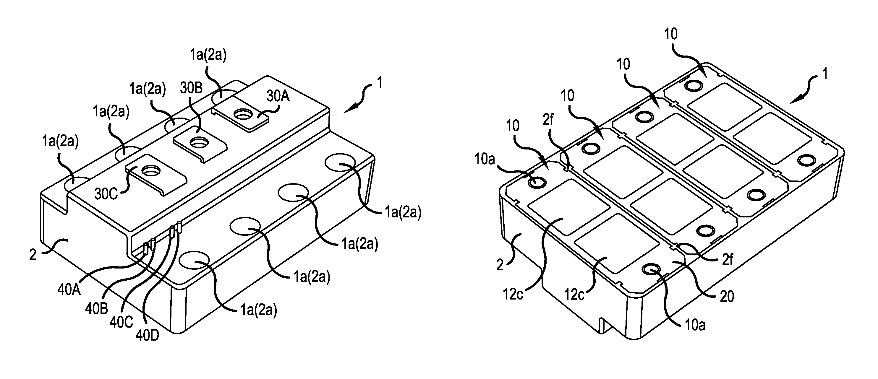
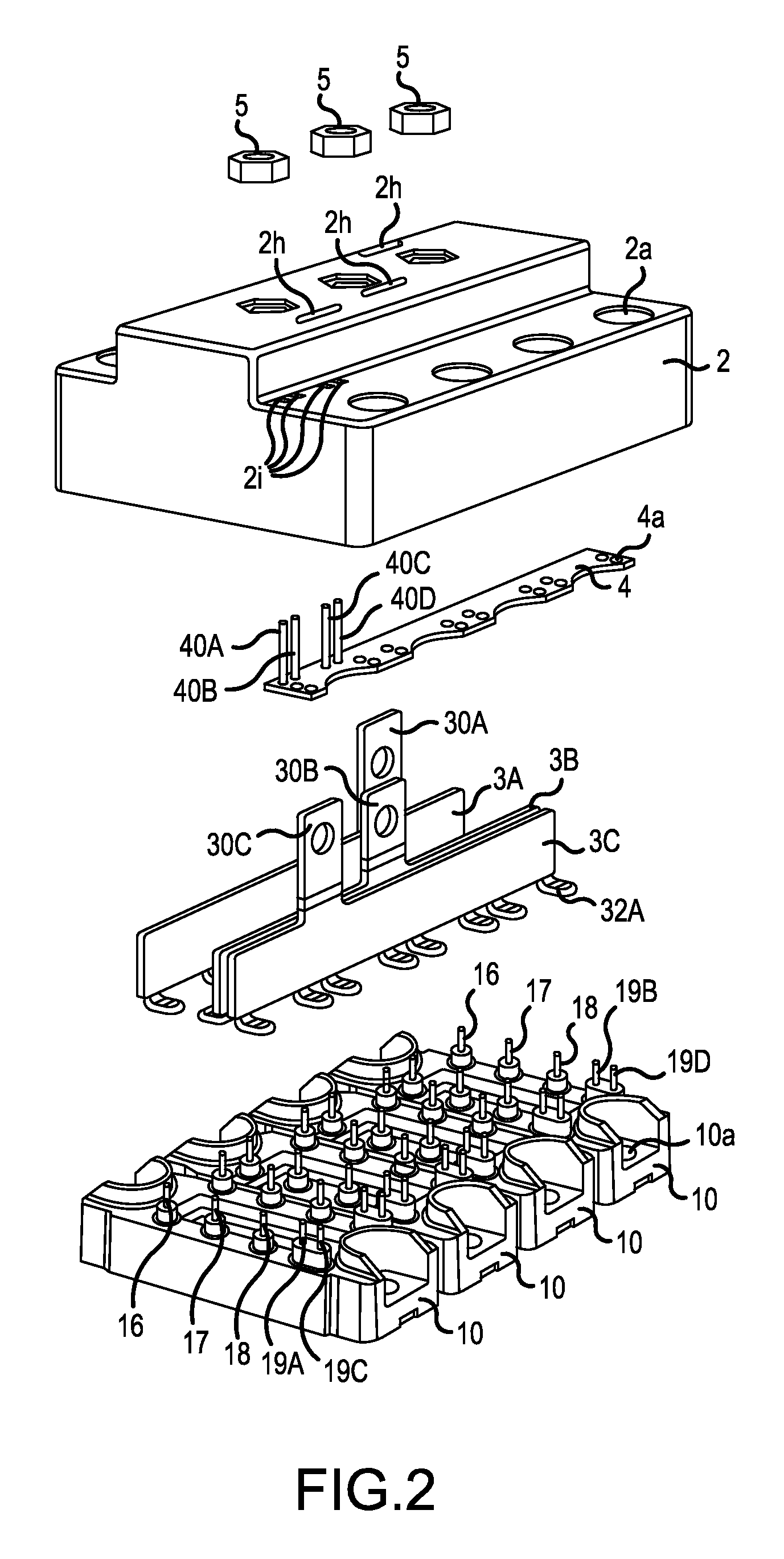
[0043]FIGS. 1A and 1B are perspective views of a semiconductor device 1 according to an embodiment of the invention, in which FIG. 1A is a view of the semiconductor device 1 seen obliquely from above, and FIG. 1B is a view of the semiconductor device 1 seen obliquely from below. As can be seen from FIG. 1B, the semiconductor device 1 comprises a multiple of (four in the example of the figure) power semiconductor modules 10 and a semiconductor module case 2 that covers and fixes the power semiconductor modules 10. As shown in FIG. 1A, the semiconductor device 1 has a configuration of a nearly rectangular parallelepiped with a side view from a shorter side having a projecting part. In the rectangular planar shape of the semiconductor device 1 of the figure, the longitudinal direction of the power semiconductor module 10 is the shor...


PUM


Abstract

A semiconductor device composed of a plurality of semiconductor modules exhibiting a large current carrying capacity for a semiconductor device as a whole is disclosed. The connection between the plurality of semiconductor modules is conducted by means of optimum construction suited to the semiconductor device. The device comprises a semiconductor module having externally connecting terminals protruding out of a casing, bus bars electrically connecting the specific externally connecting terminals of the plurality of semiconductor modules arranged in parallel with each other, and a semiconductor module case covering and fastening the plurality of semiconductor modules connected with the bus bars. The bus bars and the externally connecting terminals of the semiconductor modules are joined by means of laser welding.

Description

BACKGROUND OF THE INVENTION[0001]A. Field of the Invention[0002]The present invention relates to a semiconductor device and in particular to a semiconductor device composed of a plurality of semiconductor modules comprising power semiconductor chips, using a technique for connecting terminals of semiconductor modules.[0003]B. Description of the Related Art[0004]A power semiconductor module contains a power semiconductor chip(s), for example an insulated gate bipolar transistor(s) (IGBT(s)), mounted on an insulated circuit board and housed in a case. One type of dedicated package is prepared for power semiconductor module of a specified current carrying capacity rating. A large capacity power semiconductor module can hardly be obtained by producing a dedicated chip for a given current carrying capacity. Thus, usually employed packages have a structure which arranges in parallel a plurality of power semiconductor chips with a specified current carrying capacity.[0005]In a large capaci...

Claims


Application Information

Patent Timeline
Patent Type & Authority Patents(United States)
IPC IPC(8): H05K7/00H05K1/11H01L23/00H05K1/02H05K1/18H05K3/32
CPCH05K1/117H01L24/01H05K1/0263H01L2924/12042H01L2924/1305H01L2924/13055H01L2924/13091H05K1/181H05K3/328H05K2201/10166H05K2201/10272H05K2201/10303H01L2924/00
Inventor TADA, SHINJIMOCHIZUKI, EIJINAKAMURA, HIDEYOHORIO, MASAFUMI
Owner FUJI ELECTRIC CO LTD
Why Eureka
Try Eureka