3D nonvolatile memory device having common word line

a nonvolatile memory and word line technology, applied in semiconductor devices, semiconductor/solid-state device details, electrical devices, etc., can solve the problems of increasing the difficulty level of forming metal interconnections, difficult to ensure sufficient area, and difficult to form a large number of metal interconnections in a limited space. , to achieve the effect of improving the process margin and improving the structure of the word lin

Active Publication Date: 2016-12-06
SK HYNIX INC
View PDF7 Cites 13 Cited by
  • Summary
  • Abstract
  • Description
  • Claims
  • Application Information

AI Technical Summary

Benefits of technology

[0015]One or more exemplary embodiments are directed to improving a process margin of a 3D nonvolatile memory device by improving a structure of a word line in the 3D nonvolatile memory device.
[0018]Word lines and pass transistors may be easily coupled in the 3D nonvolatile memory devices even when the number of layers of the word lines is increased.

Problems solved by technology

However, since the word lines WL are formed in a stacking structure, it becomes difficult to form a large number of metal interconnections LWL in a limited space such as, the pass transistor region.
However, since a pitch of the cell block is not increased, a difficulty level for forming the metal interconnections increases.
In particular, it is difficult to ensure sufficient area for the pass transistor region in which one pass transistor Pass Tr is commonly coupled to the word lines of the cell regions Cell1 and Cell2 at both sides thereof.

Method used


Image

  • 3D nonvolatile memory device having common word line
  • 3D nonvolatile memory device having common word line
  • 3D nonvolatile memory device having common word line

Examples


Embodiment Construction

”.

BRIEF DESCRIPTION OF THE DRAWINGS

[0020]The above and other aspects, features and other advantages of the subject matter of the present disclosure will be more clearly understood from the following detailed description taken in conjunction with the accompanying drawings, in which:

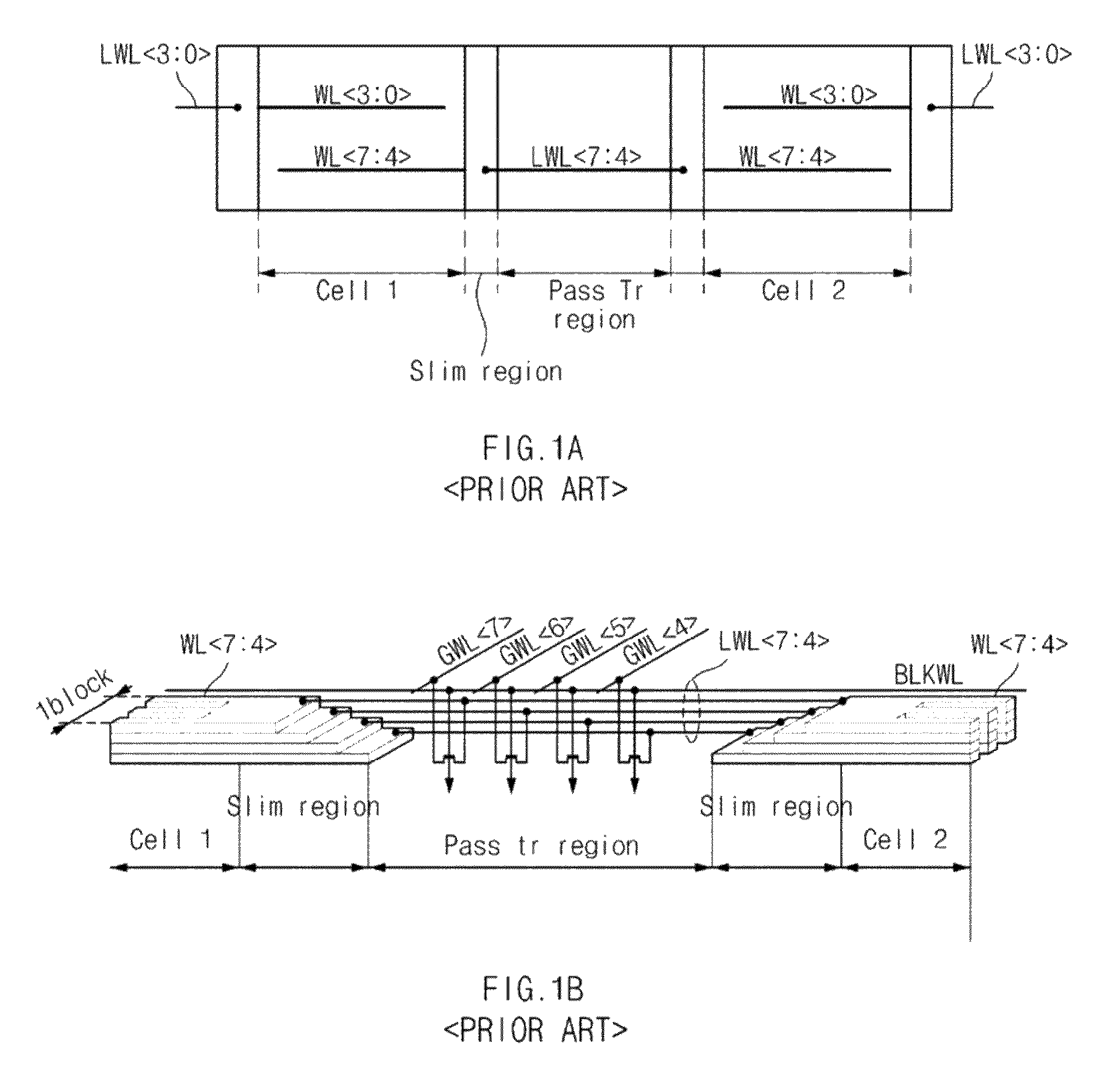
[0021]FIG. 1A and FIG. 1B are schematic views illustrating a configuration of a conventional 3D nonvolatile memory device;

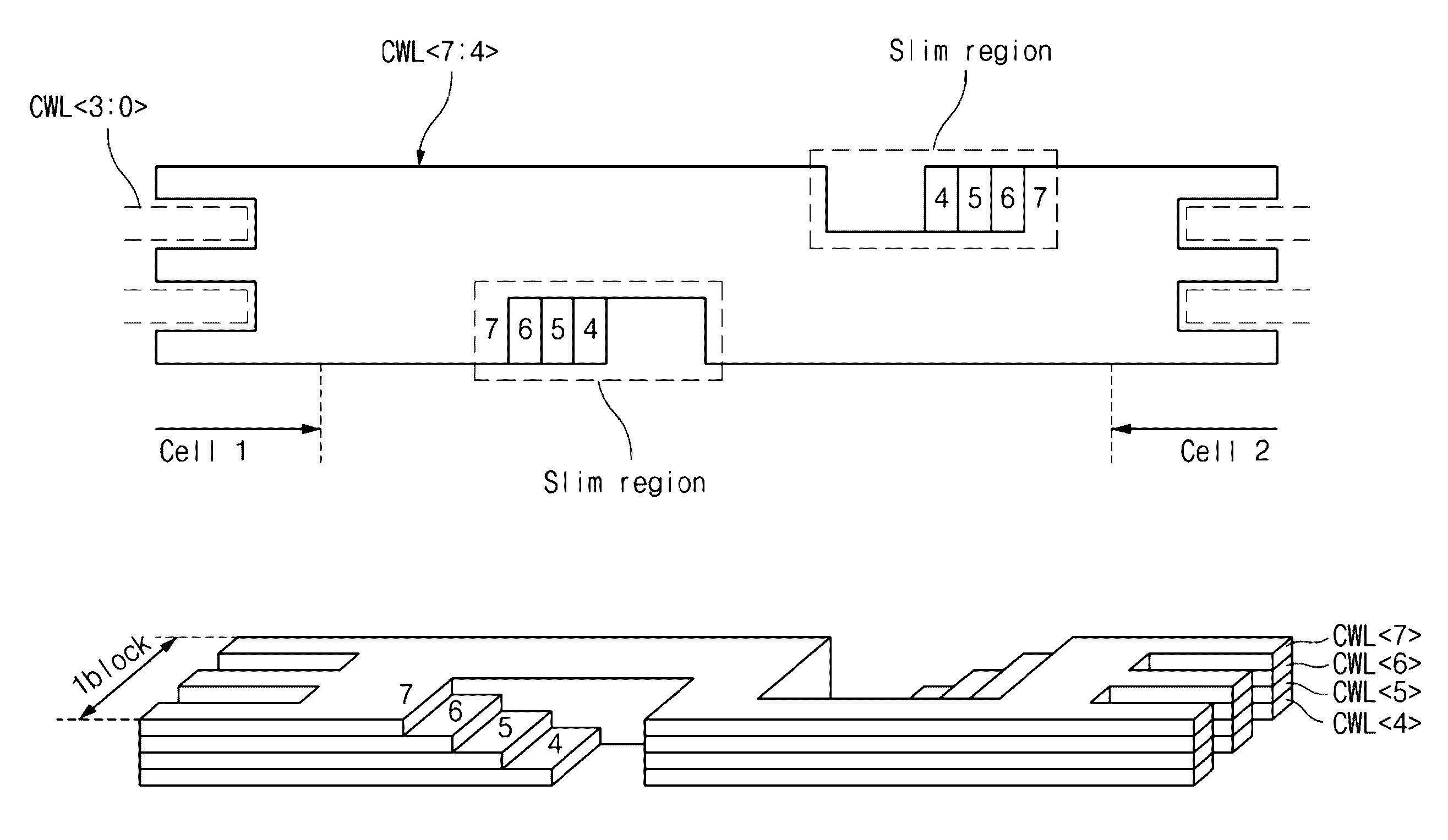
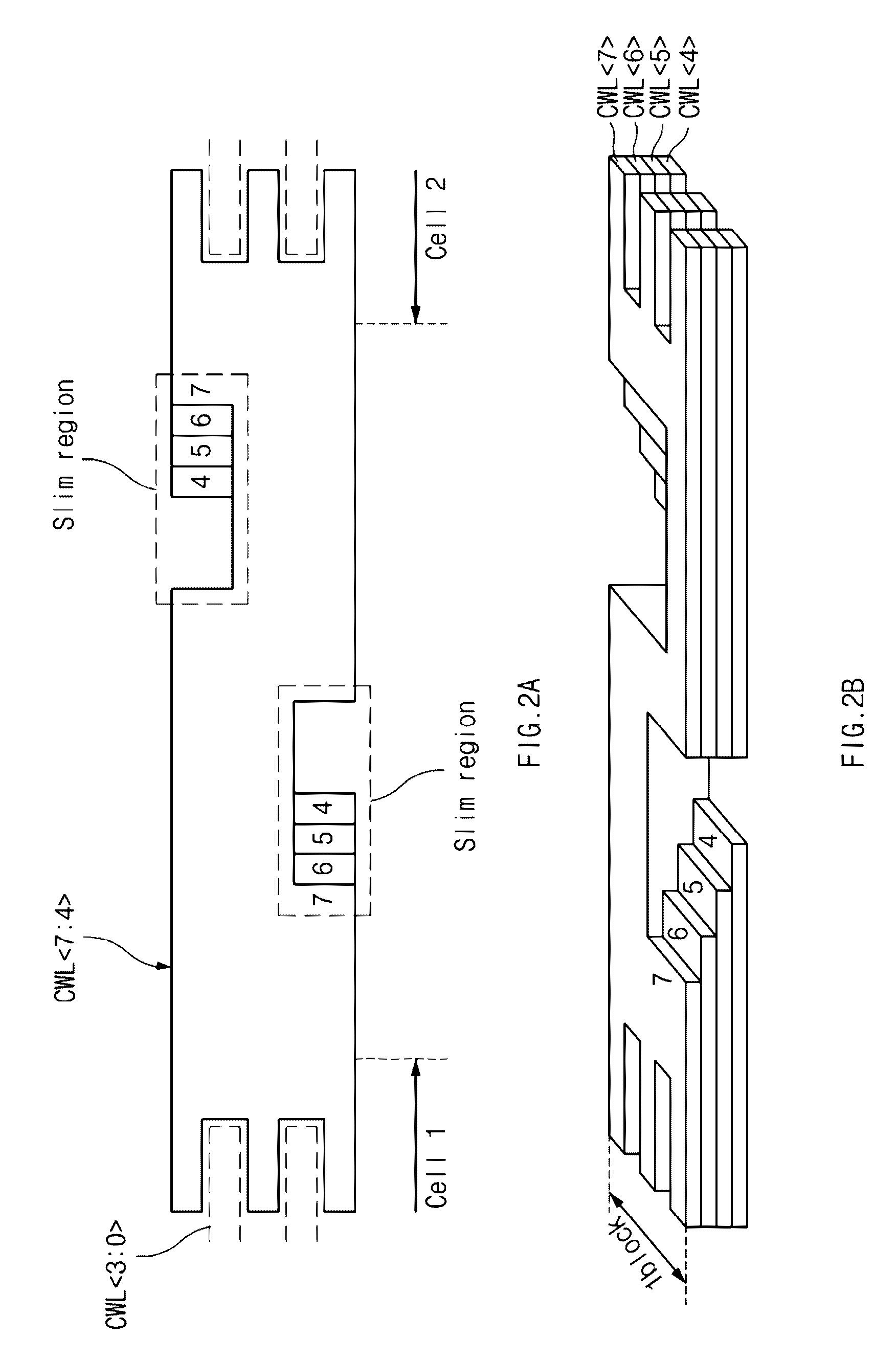
[0022]FIG. 2A and FIG. 2B are schematic views illustrating a configuration of common word lines according to an embodiment of the inventive concept;

[0023]FIGS. 3A to 3C are plan views illustrating configurations of common word lines according to other embodiments of the inventive concept;

[0024]FIGS. 4A to 4C are perspective views illustrating configurations of common word lines according to other embodiments of the inventive concept;

[0025]FIG. 5 is a view illustrating a connection relationship between common word lines and pass transistors according to an embodiment of the inventive con...


PUM


Abstract

A 3D nonvolatile memory device including memory cells vertically stacked is disclosed. Word lines are integrally formed to be elongated over adjacent cell regions spaced apart from each other, and portions of the word lines between the cell regions are partially etched in a stepped shape to form word line contact regions.

Description

CROSS-REFERENCES TO RELATED APPLICATION[0001]The present application claims priority to Korean patent application 10-2014-0140715, filed on Oct. 17, 2014, which is incorporated herein by reference in its entirety.BACKGROUND OF THE INVENTION[0002]1. Technical Field[0003]Embodiments relate to a three-dimensional (3D) nonvolatile memory device, and more particularly, to a 3D nonvolatile memory device with stacked word lines which are integrally formed, spaced apart by a given distance, and elongated over adjacent cell regions.[0004]2. Related Art[0005]Nonvolatile semiconductor memory devices are memory devices in which stored data is retained even when power is interrupted. Currently, various nonvolatile memory devices such as, flash memory devices and the like have been widely used.[0006]The flash memory devices are characterized by data programming and erasing being electrically performed. The flash memory device includes a plurality of blocks having memory cells, and each of the blo...

Claims


Application Information

Patent Timeline
Patent Type & Authority Patents(United States)
IPC IPC(8): H01L23/52H01L21/3213H01L27/115H01L21/768H01L21/76H01L21/32H01L27/11
CPCH01L27/11578H01L21/32139H01L21/768H01L27/11548H01L27/11575H01L27/11556H01L27/11582H10B41/50H10B43/50H10B41/27H10B43/27H10B43/20
Inventor OH, SUNG LAEKIM, JIN HO
Owner SK HYNIX INC
Why Eureka
Try Eureka