
Methods and structure to form high K metal gate stack with single work-function metal

a technology of work function metal and metal gate stack, which is applied in the field of metal oxide semiconductor field effect transistors, can solve the problems of poor repeatability and uniformity of process, high gate resistance, and worse variability and control of work function recess process, so as to simplify and improve the performance of the replacement metal gate stack and lower the gate resistance

Active Publication Date: 2016-12-06
TESSERA LLC
View PDF24 Cites 4 Cited by
  • Summary
  • Abstract
  • Description
  • Claims
  • Application Information

AI Technical Summary

Benefits of technology

This approach simplifies the process, achieves lower gate resistance by increasing bulk fill material, maintains correct work functions for both N-FET and P-FET, and improves repeatability and uniformity, especially at advanced node sizes below 14 nm, while reducing the number of masks required.

Problems solved by technology

Due to the number of work function materials required in current gates, the openings may be difficult to subsequently fill with the bulk material and may result in high gate resistances.
However, there are several drawbacks to work function metal recess: first, it requires several additional photolithography masks, patterning and etch steps; second, the wet etch and reactive ion etch (RIE) processes that are integral to this recess process alter the inherent work functions of the work function metals materials which remain at the bottom of the opening which leads to threshold voltage shifts; third, the repeatability and uniformity of the process is not very good, especially, with varying gate lengths of the transistors within each chip and across the entire wafer; and fourth, with the move to shorter gates (smaller vertical height of the opening) to reduce gate capacitance, the variability and control of work function recess process becomes worse.

Method used


Image

  • Methods and structure to form high K metal gate stack with single work-function metal
  • Methods and structure to form high K metal gate stack with single work-function metal
  • Methods and structure to form high K metal gate stack with single work-function metal

Examples


Embodiment Construction

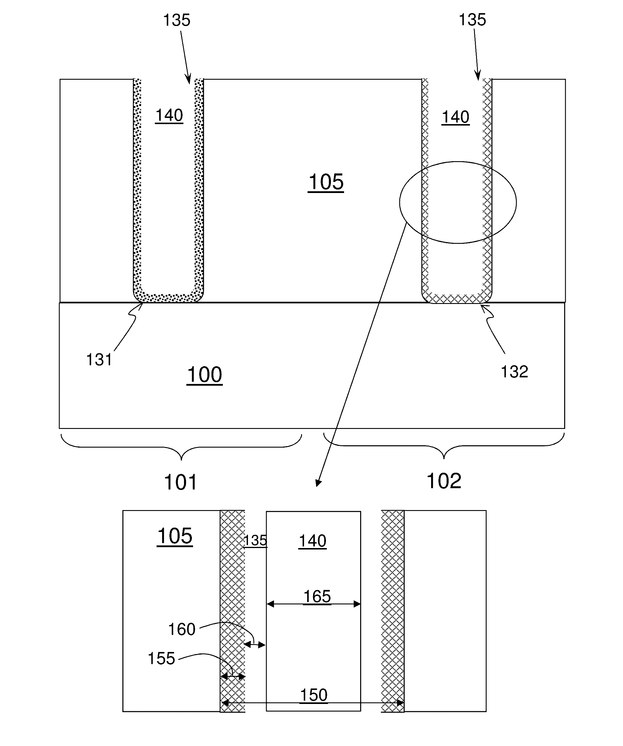
[0021]The basic principle of the invention is a method forming oppositely doped high dielectric constant replacement metal gates which have the same work function (WF) metal stack. This is in contrast to normal methods in which work function tuning of an FET is achieved by varying the WF metal materials and thicknesses of materials. Work function tuning is a way to adjust threshold voltages of a device, thus creating two work function regions which, in turn creates two threshold voltage regions.

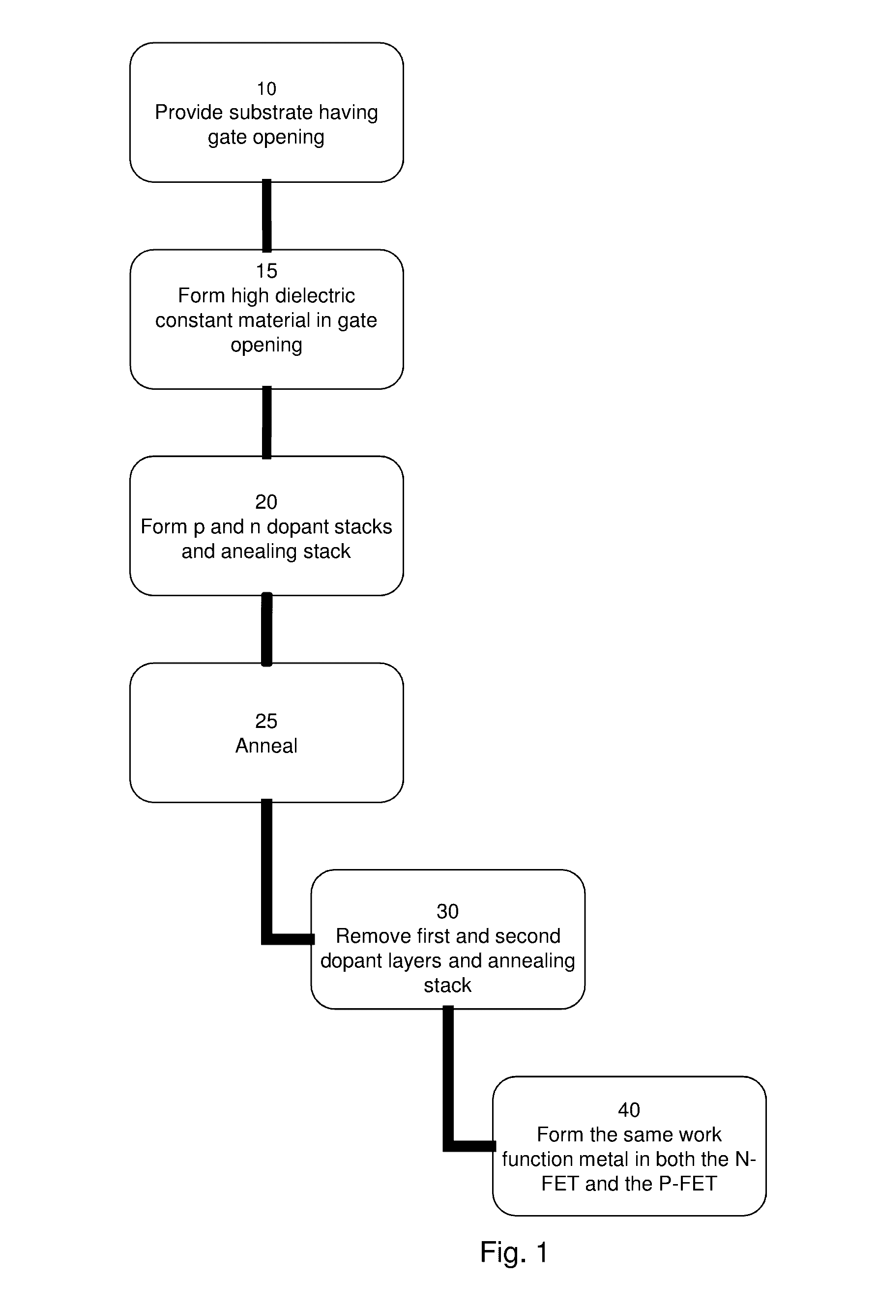
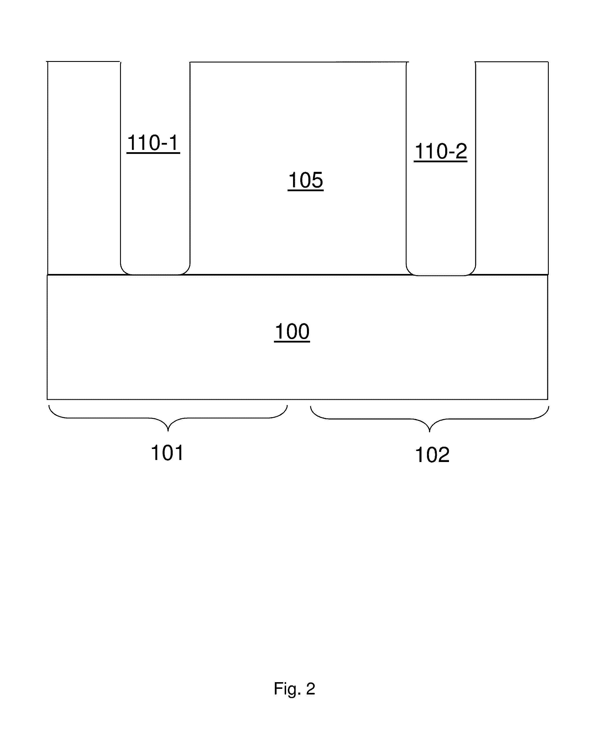
[0022]Referring to FIG. 1 a flow chart of steps to create a substrate in which the gates of oppositely doped FETs share the same WF metal according to an embodiment of the present invention is presented. In step 10, dummy gates over the N-FET and P-FET gate regions of the substrate are removed to leave gate openings (which can also be referred to as gate trenches). In step 15 a high dielectric constant material is formed in the gate openings. In step 20, p and n dopant stacks are formed as we...


PUM

PropertyMeasurementUnit
widthaaaaaaaaaa
widthaaaaaaaaaa
thicknessaaaaaaaaaa

Abstract

A method for forming a replacement metal gate structure sharing a single work function metal for both the N-FET and the P-FET gates. The method oppositely dopes a high-k material of the N-FET and P-FET gate, respectively, using a single lithography step. The doping allows use of a single work function metal which in turn provides more space in the metal gate opening so that a bulk fill material may occupy more volume of the opening resulting in a lower resistance gate.

Description

BACKGROUND OF THE INVENTION[0001]1. Field of the Invention[0002]The present invention generally relates to Metal Oxide Semiconductor Field Effect Transistors (MOSFETs) made on a semiconductor substrate. In particular, the invention relates to making MOSFETs having a single work-function metal for both the N-FET and the P-FET in a replacement metal gate structure.[0003]2. Description of Related Art[0004]In conjunction with Moore's law, gates of MOSFETs shrink with each technology node. In advanced MOSFETs, the gate may be made from a “replacement metal gate” (RMG) process which requires forming a gate opening in a dielectric layer and filling the gate opening with gate materials as opposed to patterning the gate materials and then surrounding them with a dielectric. Due to the number of work function materials required in current gates, the openings may be difficult to subsequently fill with the bulk material and may result in high gate resistances.[0005]Attempts to create more room ...

Claims


Application Information

Patent Timeline
Patent Type & Authority Patents(United States)
IPC IPC(8): H01L29/66H01L21/28H01L29/51H01L29/49H01L21/8238H01L27/092
CPCH01L21/823842H01L27/092H01L29/66545H01L21/28088H01L21/28185H01L21/28238H01L29/4966H01L29/517H01L21/225H01L21/823828H01L21/823857H01L29/42372
Inventor ANDO, TAKASHIKANNAN, BALAJIKRISHNAN, SIDDARTHKWON, UNOHSIDDIQUI, SHAHAB
Owner TESSERA LLC
Learn More