Method for forming dense silicic film

a technology of dense silicic film and silicic acid, which is applied in the direction of liquid/solution decomposition chemical coating, coating, chemical apparatus and processes, etc., can solve the problem of insufficient density of silicic film, and achieve excellent gas barrier performance

Active Publication Date: 2017-01-03
MERCK PATENT GMBH
View PDF12 Cites 1 Cited by
  • Summary
  • Abstract
  • Description
  • Claims
  • Application Information

AI Technical Summary

Benefits of technology

[0013]The present invention enables to form a dense and excellent gas barrier performance silicic film as a result of a low content of Si—O bonds and a high content of Si—N bonds.

Problems solved by technology

However, the present inventors have found that density of the film may be insufficient when irradiation light is limited to 172 nm wavelength.

Method used


Image

  • Method for forming dense silicic film
  • Method for forming dense silicic film
  • Method for forming dense silicic film

Examples


Embodiment Construction

.

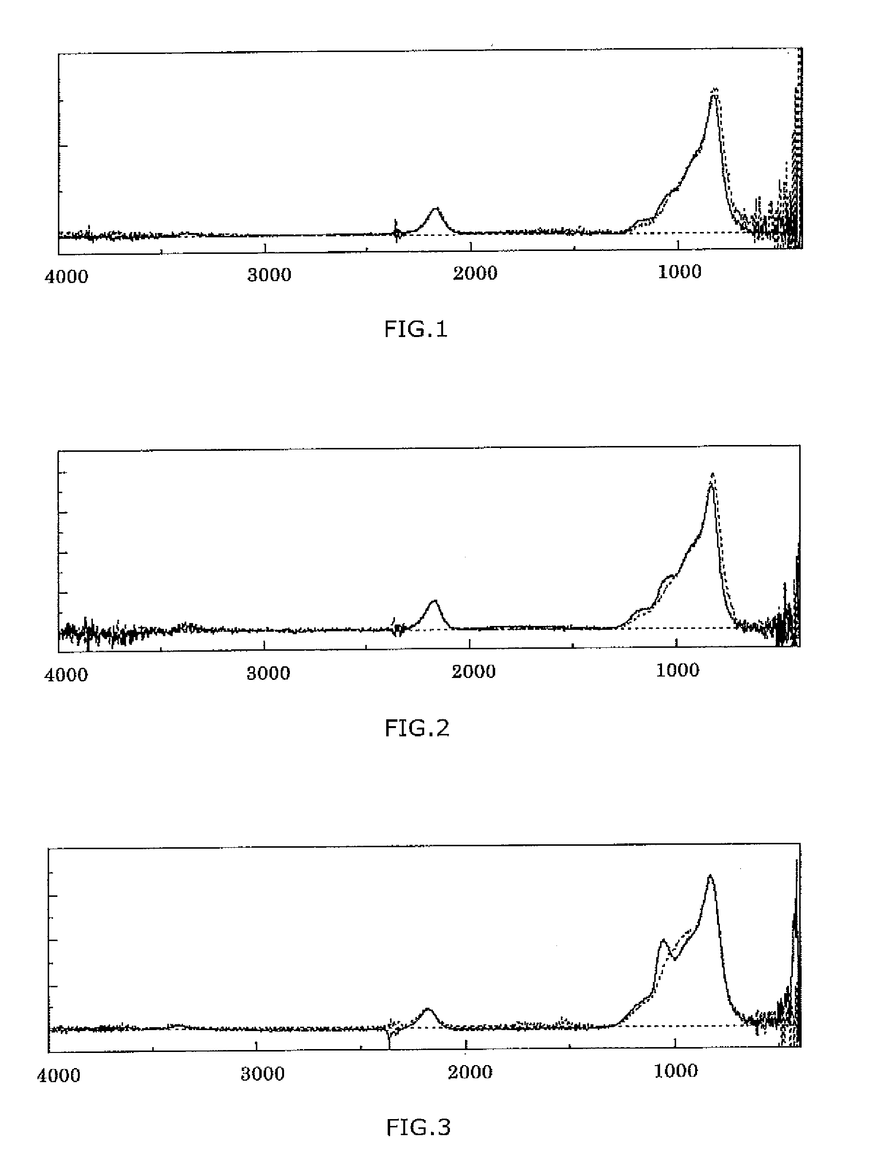
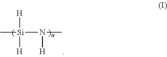
[0015]FIG. 2 is IR spectra after irradiation process (broken line) and after superheated steam process (solid line) at Example 1.

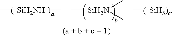
[0016]FIG. 3 is IR spectra after irradiation process (broken line) and after superheated steam process (solid line) at Example 37.

BEST MODE FOR CARRYING OUT THE INVENTION

[0017]Embodiments of the present invention are described in detail.

[0018]In the present invention, a dense silicic film is provided on one or both sides of a substrate. The substrate is not limited and can be freely selected from metallic materials, ceramics and organic materials. Specifically, a bare silicon wafer and a silicon wafer coated with, for example, a thermal oxide film can be used. A dense silicic film can be formed on not only one side but also both sides of a substrate. In this case, a substrate should be selected according to the intended use.

[0019]In a method for forming a gas barrier film according to the present invention, a substrate surface is coated with a composition...


PUM

PropertyMeasurementUnit
wavelengthaaaaaaaaaa
maximal peak wavelengthaaaaaaaaaa
wavelengthaaaaaaaaaa

Abstract

The present invention provides a dense silicic film and a producing method thereof. This method comprises coating a composition for coating film, which comprises a polymer having a silazane bond on a substrate, on a substrate, irradiating with light having a maximal peak in the range of 160-179 nm wavelength, and then irradiating with light having 10-70 nm wavelength longer maximal peak wavelength than the light used in the previous irradiation.

Description

[0001]This application is a United States National Stage Patent Application under 35 U.S.C. §371 of International Patent Application No. PCT / JP2013 / 077487, filed Oct. 9, 2013, which claims priority to Japanese Patent Application No. 2012-226078, filed Oct. 11, 2012, the contents of which are being hereby incorporated herein by reference.TECHNICAL FIELD[0002]The present invention relates to methods for producing silicic dense film, which can be used for manufacturing semiconductor devices.BACKGROUND ART[0003]Silicic films, which are relatively hard and dense, are used in various applications, specifically a hard-coat film, a gas barrier film and a reinforcement film for substrates and circuits and the like in the semiconductor manufacturing industry. Various silicic films for such applications have been investigated. Non-Patent Document 1 discloses a method for forming a SiON layer by coating polysilazane on a substrate, drying, and then irradiating with excimer laser (wavelength 172...

Claims


Application Information

Patent Timeline
Patent Type & Authority Patents(United States)
IPC IPC(8): B05D3/06C08J7/12C08J7/04C09D183/16C23C18/12C08J7/00C01B21/068C23C18/14C08J7/048
CPCC09D183/16B05D3/067C01B21/068C08J7/00C08J7/047C08J7/123C23C18/122C23C18/1233C23C18/1241C23C18/1245C23C18/14C08J2483/16C08J7/0427C08J7/048
Inventor OZAKI, YUKISAKURAI, TAKAAKIKOBAYASHI, MASAKAZU
Owner MERCK PATENT GMBH
Why Eureka
Try Eureka