Solid-state image sensor and camera with charge-voltage converter

a solid-state image sensor and charge-voltage converter technology, which is applied in the field of solid-state image sensors and cameras, can solve the problems of limited charge quantity that can be transferred to the fd serving as the charge-voltage converter, and achieve the effect of widening the dynamic range and increasing the charge quantity

Active Publication Date: 2017-01-03
CANON KK
View PDF42 Cites 24 Cited by
  • Summary
  • Abstract
  • Description
  • Claims
  • Application Information

AI Technical Summary

Benefits of technology

[0006]The present invention provides a solid-state image sensor having an arrangement advantageous in increasing a charge quantity that can be transferred to a charge-voltage converter and widening a dynamic range.

Problems solved by technology

Therefore, the charge quantity that can be transferred to the FD serving as the charge-voltage converter is limited to be in the range where the reset transistor is not turned on.

Method used


Image

  • Solid-state image sensor and camera with charge-voltage converter
  • Solid-state image sensor and camera with charge-voltage converter
  • Solid-state image sensor and camera with charge-voltage converter

Examples


first embodiment

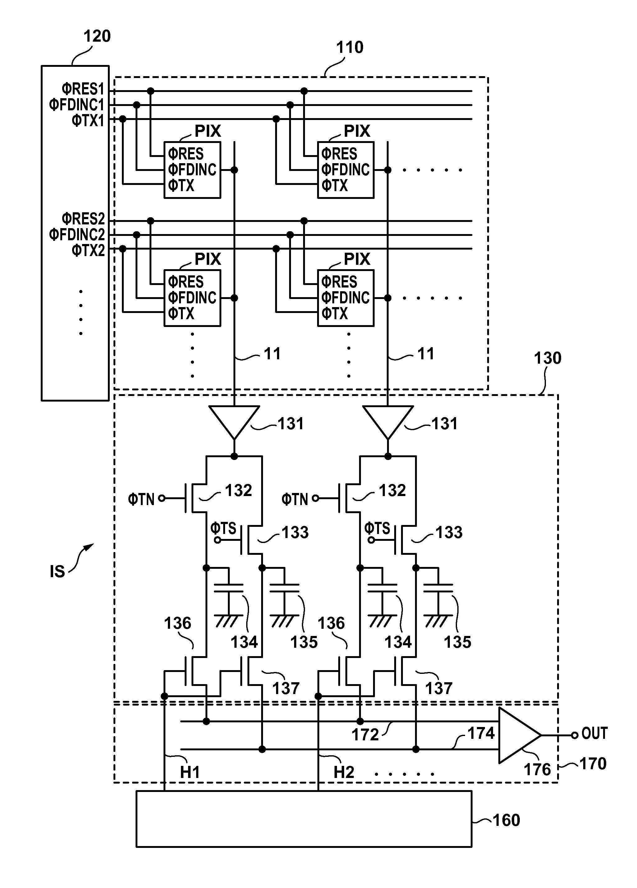
[0016]The circuit arrangement of a solid-state image sensor IS according to the present invention will be described with reference to FIG. 1. The solid-state image sensor IS includes a pixel array 110 in which a plurality of pixels PIX are arrayed to form a plurality of rows and a plurality of columns, and a readout unit 130 which reads out the signal of each pixel PIX from the pixel array 110. The solid-state image sensor IS also includes a row selection unit (control unit) 120 which selects a read target row in the pixel array 110, a column selection unit 160 which selects the signals read out by the readout unit 130, and an output unit 170 which outputs the signals selected by the column selection unit 160.

[0017]The row selection unit (control unit) 120 outputs a reset signal φRES, an extension signal φFDINC, and a transfer signal φTX. The reset signal φRES supplied to the ith row is denoted as φRESi (for example, φRES1 or φRES2). Similarly, the extension signal φFDINC supplied t...

third embodiment

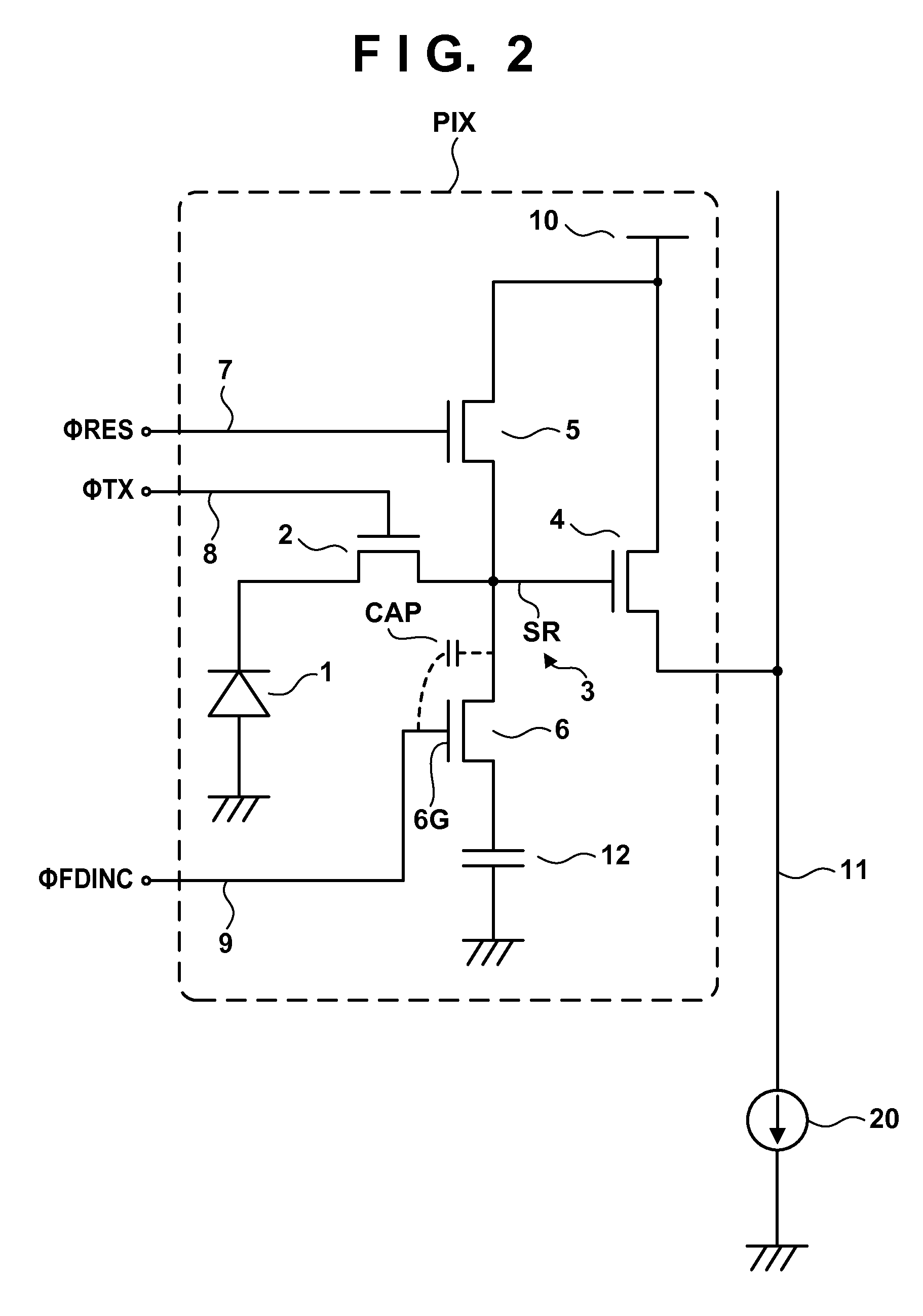
[0040]If the electrode 6G′ is driven to high level, electrons move to the surface region of a semiconductor substrate SUB under the electrode 6G′, thereby forming an inversion layer SS like a channel in the MOS transistor, and a additional capacitance 12 is formed as the parasitic capacitance of the inversion layer SS. By forming the inversion layer SS, a capacitance value that can be seen from the gate of an amplifier transistor 4 will be a value obtained by adding the capacitance value of the additional capacitance 12 to the capacitance value of a charge-voltage converter 3. In the third embodiment, since the additional capacitance 12 is formed by the formation of the inversion layer SS and disappears by the disappearance of the inversion layer SS, the reset of the additional capacitance 12 is unnecessary.

[0041]The second semiconductor region SR2′ may be replaced by an element isolation ISO. In this case, a process of forming the second semiconductor region SR2′ in the formation r...


PUM


Abstract

An image sensor including a photoelectric converter, a charge-voltage converter, a transfer transistor to transfer a charge from the photoelectric converter to the charge-voltage converter whereby potential of the charge-voltage converter changes to a first direction, an amplifier transistor to output a signal corresponding to potential of the charge-voltage converter to a column signal line, the amplifier transistor sequentially outputting, to the column signal line, noise level and light signal level, a capacitance between a control signal line and the charge-voltage converter, and a control unit to change a potential of the control signal line so that the potential of the charge-voltage converter changes to a second direction opposite to the first direction in a period in which the charge-voltage converter is in floating and which is prior to outputting the noise level.

Description

BACKGROUND OF THE INVENTION[0001]Field of the Invention[0002]The present invention relates to a solid-state image sensor and a camera.[0003]Description of the Related Art[0004]A solid-state image sensor including a plurality of two-dimensionally arrayed photoelectric converters is mounted in a digital camera, a digital camcorder, or the like. In the solid-state image sensor, a transfer transistor transfers charges accumulated in the photoelectric converters to a floating diffusion (to be referred to as an FD hereinafter). The FD functions as a charge-voltage converter which converts a charge quantity into a voltage. The gate of an amplifier transistor is connected to the FD. The amplifier transistor outputs, to a column signal line, a signal corresponding to the charge quantity (the potential of the FD) transferred to the FD. The charge quantity that can be transferred to the FD depends on the potential of the FD. Japanese Patent Laid-Open No. 2012-010106 describes that when the FD ...

Claims


Application Information

Patent Timeline
Patent Type & Authority Patents(United States)
IPC IPC(8): H04N5/378H04N5/355
CPCH04N5/378H04N5/3559H04N25/59H04N25/75
Inventor WADA, YOICHIKOBAYASHI, MASAHIROINUI, FUMIHIRO
Owner CANON KK
Why Eureka
Try Eureka