Multi-layer printed circuit boards with dimensional stability

a printed circuit board and dimensional stability technology, applied in the direction of printed circuit manufacturing, printed circuit stress/warp reduction, printed circuit aspects, etc., can solve the problems of increasing production costs, and achieve the effects of high signal transmission property material, high dimensional stability material, and increased dimensional stability of multi-layer boards

Active Publication Date: 2017-01-10
ELITE MATERIAL
View PDF39 Cites 2 Cited by
  • Summary
  • Abstract
  • Description
  • Claims
  • Application Information

AI Technical Summary

Benefits of technology

[0041]A primary advantage of the present invention is using a high dimensional stability material as the core layer to increase the dimensional stability of a multi-layer board in subsequent processes and using a high signal transmission property material as other insulation layers (a.k.a. dielectric layers) to effectively increase the signal transmission speed, thereby overcoming at the same time the following three problems associated to a multi-layer printed circuit board architecture: (A) poor dimensional stability and poor signal transmission speed of multi-layer boards using ordinary FR-4 material; (B) poor dimensional stability of multi-layer boards using ordinary low Dk material; (C) low signal transmission speed of multi-layer boards using high dimensional stability material, as materials with high dimensional stability usually have higher dielectric constant, and other problems associated to high material costs, demand for higher lamination temperature and the accompanying higher lamination costs, poor thermal resistance of copper foil after brown oxidation, and poor processability for routing and trimming.

Problems solved by technology

If the lamination process causes severe deformation, the final products won't be able to meet the requirements and have to be discarded, which will increase the production costs.

Method used


Image

  • Multi-layer printed circuit boards with dimensional stability
  • Multi-layer printed circuit boards with dimensional stability
  • Multi-layer printed circuit boards with dimensional stability

Examples


embodiments

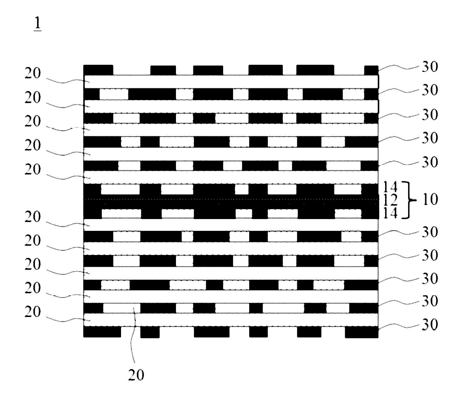
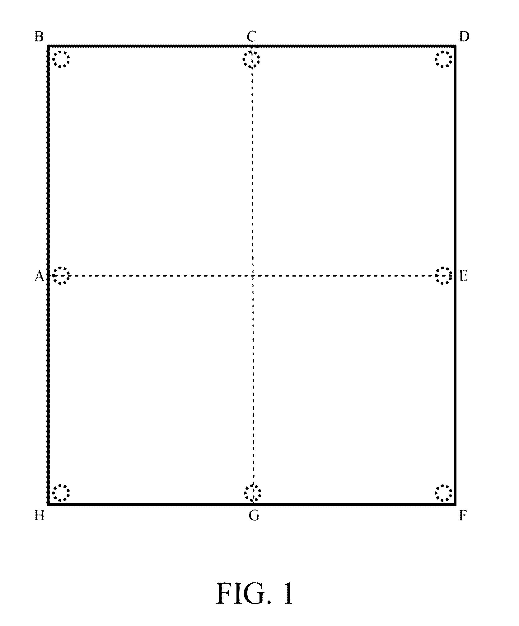
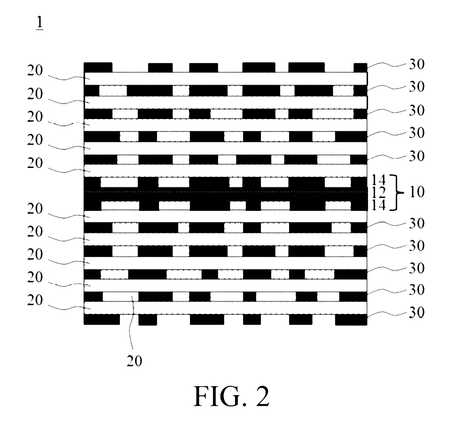
[0042]The core of Example 1 is made by the following process: preparing a first prepreg (EM-LX, available from Elite Material Co., Ltd., containing 1078 glass fiber cloth), superimposing a 0.5 oz HTE copper foil on each of two sides of the first prepreg and carrying out lamination for three hours under vacuum, high temperature (195° C.) and high pressure (500 psi) to obtain a copper-clad laminate, and fabricating traces, such as using conventional exposure, lithography and etching processes, on the copper foil to obtain the core. The traces are designed according to a Gerber artwork (24.3 inches in length (Y) and 20.3 inches in width (X)), where locations for eight target points for alignment are designed, and correspondingly eight target points are formed on the core by trace etching and used as the reference for measuring the deformation of the board in the subsequent lamination process. The distribution of target points A to H is illustrated in FIG. 1, wherein the distance betwee...


PUM

PropertyMeasurementUnit
glass transition temperatureaaaaaaaaaa
storage modulusaaaaaaaaaa
dielectric constantaaaaaaaaaa

Abstract

A multi-layer printed circuit board comprises: a core comprising a core insulation layer and traces formed on two sides of the core insulation layer; a plurality of insulation layers sequentially formed at two sides of the core; and a plurality of trace layers respectively formed between two insulation layers and on the outmost insulation layers; wherein the core insulation layer contains a resin material different from that of the insulation layers, such that the core insulation layer has a dimensional stability superior to that of the insulation layers.

Description

CROSS-REFERENCE TO RELATED APPLICATIONS[0001]This Application claims priority of Taiwan Patent Application No. 103138278, filed on Nov. 5, 2014, the entirety of which is incorporated by reference herein.FIELD OF THE INVENTION[0002]The present invention relates to multi-layer printed circuit boards and more particularly to multi-layer printed circuit boards with high dimensional stability and excellent signal transmission property.BACKGROUND OF THE INVENTION[0003]In order to meet the demands of compact, light-weight and conveniently portable electronic products, research and development of electronic product manufacturers are directed to and focused on miniaturization of electronic components.[0004]Printed circuit boards are one of the essential components of many electronic products, such as smart phones, and served to provide electronic signal transmission among different electronic components. Several technical solutions have been proposed, such as high density interconnection (HD...

Claims


Application Information

Patent Timeline
Patent Type & Authority Patents(United States)
IPC IPC(8): H05K1/03H05K3/46
CPCH05K3/4602H05K1/0366H05K2201/029H05K2201/068H05K1/0271H05K1/09H05K3/4652H05K2201/0355
Inventor KUO, YA-WENYU, LI-CHIHHO, CHING-HSIN
Owner ELITE MATERIAL
Why Eureka
Try Eureka