Plasma processing apparatus and plasma processing method

a processing apparatus and plasma technology, applied in the direction of chemical vapor deposition coating, coating, electric discharge tube, etc., can solve the problems of lowering the voltage, less easy to fulfill the plasma ignition, and the dielectric so as to achieve stable plasma ignition and suppress the breakdown of the dielectric member

Active Publication Date: 2017-02-28
PANASONIC INTELLECTUAL PROPERTY MANAGEMENT CO LTD
View PDF44 Cites 7 Cited by
  • Summary
  • Abstract
  • Description
  • Claims
  • Application Information

AI Technical Summary

Benefits of technology

[0007]In the plasma processing apparatuses described in JP 2013-120633 A, JP 2013-120684 A and JP 2013-120685 A, the chamber is defined by a dielectric member (i.e., the chamber is surrounded by a dielectric member). Also, a dielectric member for defining a chamber is placed between a high-potential conductor member and a low-potential conductor member. As a result of this, raising the voltage fed to the conductor members to enhance the plasma processing performance (heating performance) may cause the dielectric member to yield dielectric breakdown.
[0008]It could be conceived to lower the voltage applied to the conductor members for suppression of the dielectric breakdown of the dielectric member. However, lowering the voltage may make it less easy to fulfill the plasma ignition.
[0009]Therefore, an object of the present disclosure is to provide a plasma processing apparatus and method capable of fulfilling stable plasma ignition and suppressing dielectric breakdown of the dielectric member that defines the chamber.

Problems solved by technology

As a result of this, raising the voltage fed to the conductor members to enhance the plasma processing performance (heating performance) may cause the dielectric member to yield dielectric breakdown.
However, lowering the voltage may make it less easy to fulfill the plasma ignition.

Method used


Image

  • Plasma processing apparatus and plasma processing method
  • Plasma processing apparatus and plasma processing method
  • Plasma processing apparatus and plasma processing method

Examples


embodiment 1

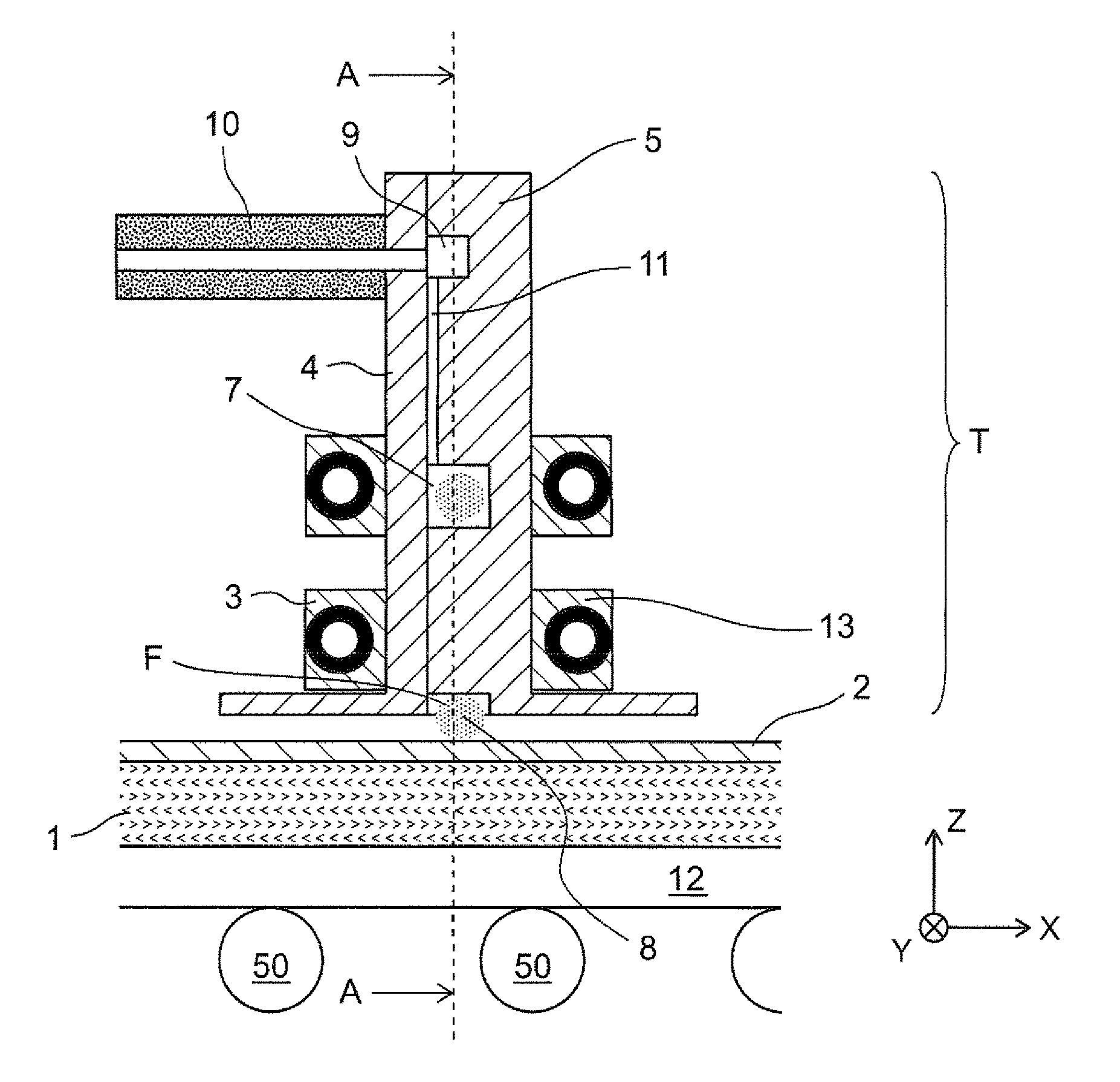
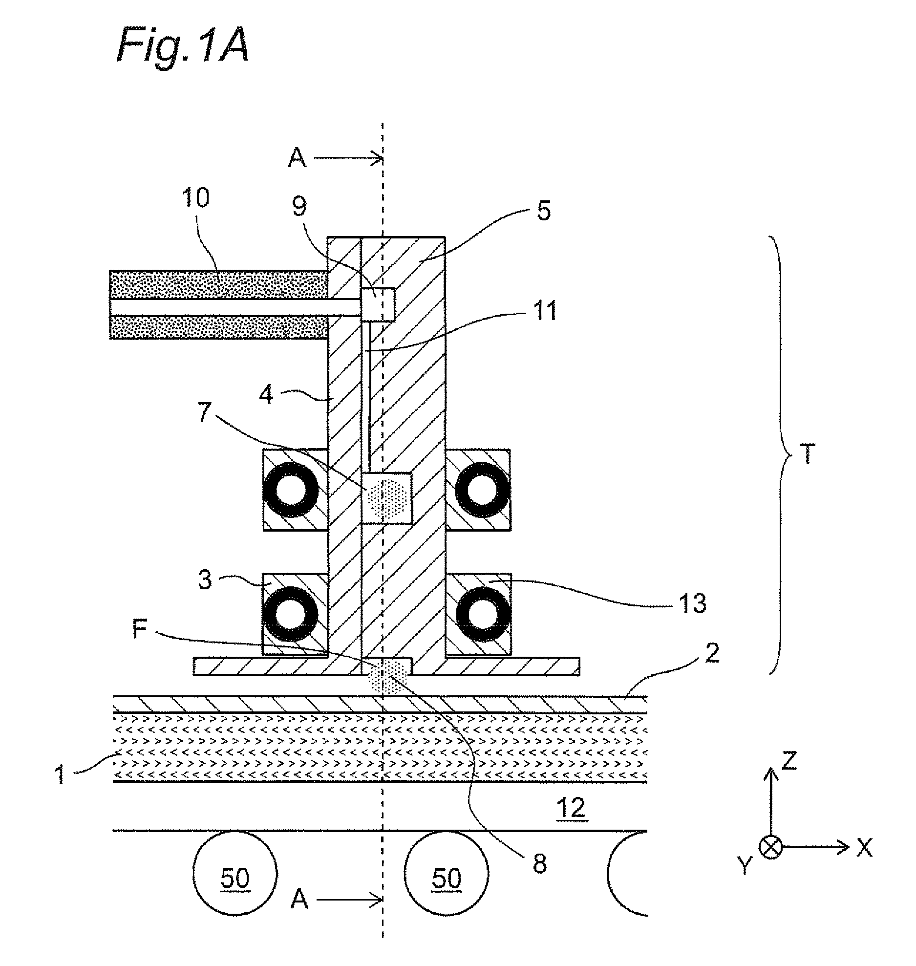
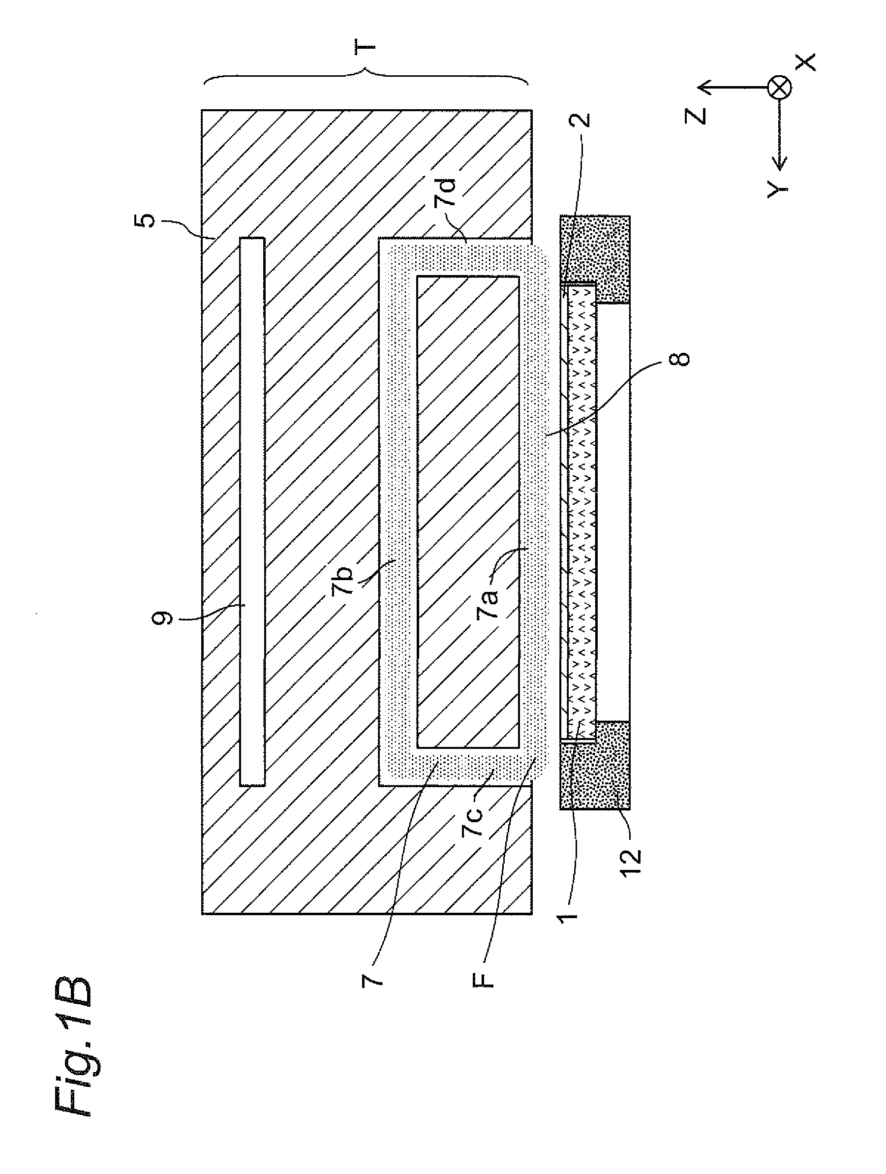
[0053]A plasma processing apparatus according to Embodiment 1 of the disclosure will be described with reference to FIGS. 1 to 4.

[0054]FIG. 1A is a sectional view which schematically shows a construction of a plasma processing apparatus according to Embodiment 1 of the disclosure and, more specifically, as will be described in detail later, which shows a cross section perpendicular to a longitudinal direction (Y-axis direction) of an opening of an inductively coupled plasma torch unit in the plasma processing apparatus. Also, FIG. 1B is a sectional view which is parallel to the longitudinal direction (Y-axis direction) of the opening of the inductively coupled plasma torch unit and which is perpendicular to a substrate that is to be plasma processed. That is, FIG. 1B shows a cross section taken along the line A-A shown in FIG. 1A. FIG. 2 is an exploded view of the inductively coupled plasma torch unit shown in FIGS. 1A and 1B.

[0055]FIGS. 1A and 1B also show an inductively coupled pl...

embodiment 2

[0123]Embodiment 2 of the disclosure will be described below with reference to FIG. 5. It is noted that the plasma torch unit T and the matching circuit 18 are identical in construction to those of the above-described Embodiment 1.

[0124]FIG. 5 is a perspective view showing electrical connections for the plasma torch unit T according to this Embodiment 2.

[0125]As shown in FIG. 5, one end 14 of the first discharge coil 3 is connected to an output terminal 20 of the matching circuit 18. The other end 15 of the first discharge coil 3 is connected to the other end 17 of the second discharge coil 13 via a high-voltage generating capacitor 25. The high-voltage generating capacitor 25 is a variable capacitor. One end 16 of the second discharge coil 13 is grounded.

[0126]In addition, the one end 16 of the second discharge coil 13 may be non-grounded. A conductor member facing the first discharge coil 3 may be not the second discharge coil 13 but a conductor member of some other shape such as ...

embodiment 3

[0140]Embodiment 3 of the disclosure will be described below with reference to FIG. 6. It is noted that the plasma torch unit T and the matching circuit 18 are identical in construction to those of the above-described Embodiment 1.

[0141]FIG. 6 is a perspective view showing electrical connections for the plasma torch unit T according to Embodiment 3 of the disclosure. As shown in FIG. 6, one end 14 of the first discharge coil 3 is connected to an output terminal 20 of the matching circuit 18. The other end 15 of the first discharge coil 3 is grounded via a high-voltage generating coil 26. The high-voltage generating coil 26 is a variable inductor. One end 16 of the second discharge coil 13 is grounded, while the other end 17 of the second discharge coil 13 is electrically floating. Instead, the other end 17 of the second discharge coil 13 may be grounded. Also, the second discharge coil 13 may be non-grounded. Further, instead of the second discharge coil 13, a conductor member of so...


PUM

PropertyMeasurementUnit
frequencyaaaaaaaaaa
frequencyaaaaaaaaaa
temperatureaaaaaaaaaa

Abstract

The plasma processing apparatus includes a dielectric member for defining a chamber, a gas introducing part for introducing a gas into the chamber, a discharge coil disposed on one side of the dielectric member and supplied with AC power to generate a plasma in the chamber into which the gas has been introduced, a conductor member disposed on the other side of the dielectric member and facing the discharge coil with the chamber of the dielectric member interposed therebetween, an AC power source for supplying AC voltage to the discharge coil, an opening communicating with the chamber and serving for applying the plasma to a substrate to be processed, and a moving mechanism for moving the substrate relative to the chamber so that the substrate passes across a front of the opening. The discharge coil is grounded or connected to the conductor member via a voltage generating capacitor or a voltage generating coil.

Description

CROSS-REFERENCE TO RELATED APPLICATIONS[0001]The present application is a priority claim application based on Japanese Patent Applications No. 2013-170097 filed to Japanese Patent Office on Aug. 20, 2013 and No. 2014-61808 filed to Japanese Patent Office on Mar. 25, 2014. The entire disclosures of these Japanese Patent Applications, including specification, claims, drawings, and summary are incorporated herein by reference in their entirety.TECHNICAL FIELD[0002]The present disclosure relates to a plasma processing apparatus and a plasma processing method for applying plasma irradiation to process a substrate or the like.BACKGROUND ART[0003]Conventionally, poly-Si (polysilicon) or other semiconductor thin films are widely used for TFTs (Thin Film Transistors) and solar cells. A method for formation of those semiconductor thin films with low cost is one in which an amorphous silicon film is irradiated with laser light so as to be crystallized. Laser process can be applied also to, for...

Claims


Application Information

Patent Timeline
Patent Type & Authority Patents(United States)
IPC IPC(8): C23C16/00C23F1/00H01L21/306H01J37/32
CPCH01J37/321H01J37/32119H01J37/32935H01J37/3211H01J37/32174
Inventor OKUMURA, TOMOHIRO
Owner PANASONIC INTELLECTUAL PROPERTY MANAGEMENT CO LTD
Why Eureka
Try Eureka