Imaging device, imaging apparatus, electronic apparatus, threshold value calculation apparatus, and imaging method

a threshold value calculation and imaging device technology, applied in the field of imaging devices, can solve the problems of relatively expensive photomultiplier tubes, and achieve the effect of improving the accuracy of a decision on a photon incident on a pixel and excellent

Active Publication Date: 2017-03-21
SONY SEMICON SOLUTIONS CORP
View PDF11 Cites 9 Cited by
  • Summary
  • Abstract
  • Description
  • Claims
  • Application Information

AI Technical Summary

Benefits of technology

[0022]The present technology can achieve an excellent effect that the accuracy of a decision on a photon incident on a pixel can be improved.

Problems solved by technology

In such an apparatus, a photomultiplier tube, which is relatively expensive, is used as a detection unit of faint light in many cases.

Method used


Image

  • Imaging device, imaging apparatus, electronic apparatus, threshold value calculation apparatus, and imaging method
  • Imaging device, imaging apparatus, electronic apparatus, threshold value calculation apparatus, and imaging method
  • Imaging device, imaging apparatus, electronic apparatus, threshold value calculation apparatus, and imaging method

Examples


first embodiment

1. First Embodiment

A Configuration Example of an Imaging Device

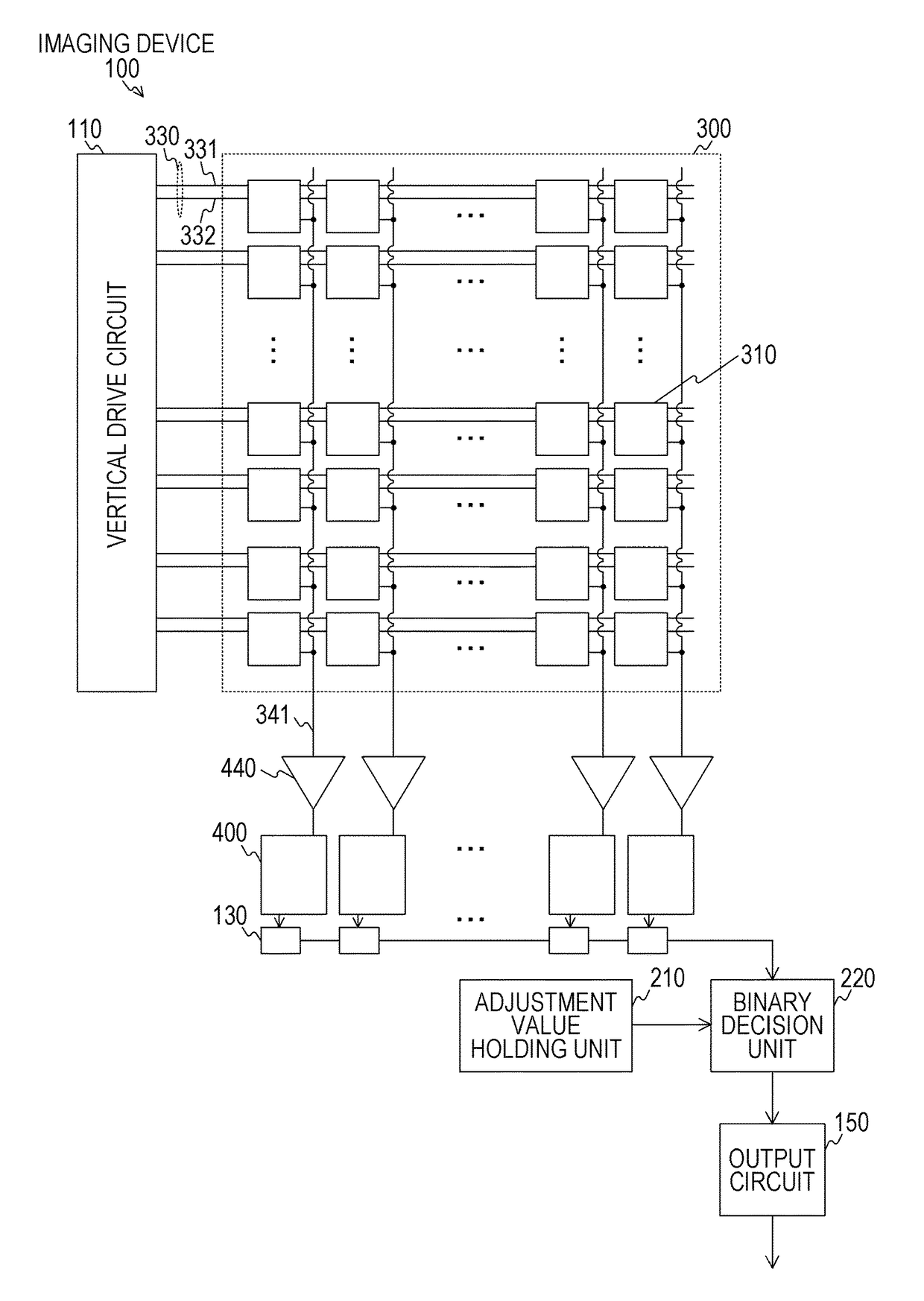
[0048]FIG. 1 is a conceptual diagram illustrating an example of a basic configuration example of an imaging device 100 of a first embodiment of the present technology.

[0049]The imaging device 100 is a photodetector provided to a system for detecting faint light (for example, a fluorescence scanner of an imaging plate, and a radiation scintillation counter). The imaging device 100 is fabricated of, for example, a CMOS (Complementary Metal Oxide Semiconductor) sensor. The imaging device 100 is used instead of a known photomultiplier tube, avalanche photodiode, photodiode, or the like.

[0050]The imaging device 100 includes a pixel array unit 300, a vertical drive circuit 110, an amplifier unit 440, a digital value generation circuit 400, a resistor 130, an adjustment value holding unit 210, a binary decision unit 220, and an output circuit 150.

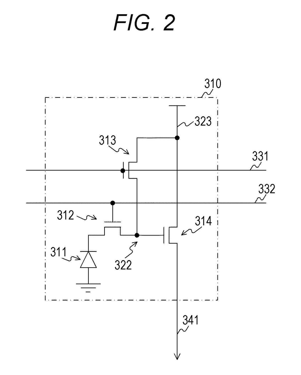
[0051]The pixel array unit 300 includes a plurality of pixels (pixels 310) arrange...

effect examples

[0153]FIGS. 7a and 7b are diagrams schematically illustrating the effect of making a binary decision using a pixel-specific adjustment value held by the adjustment value holding unit 210 of the first embodiment of the present technology.

[0154]FIG. 7a illustrates an example that assumes that a binary decision is made with one threshold value for all the pixels in the imaging device where gain varies according to each pixel (an example where a single threshold value is set for all the pixels).

[0155]FIG. 7a illustrates two graphs respectively illustrating the frequency distributions of output signals of two pixels (a pixel A and a pixel B) having different gains. In the two graphs, when the vertical axis is an axis indicating frequency, and the horizontal axis is an axis indicating the amount of signal (the gradation value of the digital value), the frequency distributions are illustrated of a signal generated in a state where there is no charge stored (a no-storage signal) and a signa...

second embodiment

2. Second Embodiment

[0320]In the first embodiment, the adjustment apparatus 550 obtains a threshold value from no-storage signals of an unexposed signal. However, the adjustment apparatus 550 can also obtain a threshold value from signals of an exposed pixel. The adjustment apparatus 550 of a second embodiment is different from that of the first embodiment in that a threshold value is obtained from signals of an exposed pixel.

[0321]FIG. 21 is a graph illustrating an example of the relationship between the standard deviation and average value of digital values in the second embodiment of the present technology. As described above, the signal amount (gradation value) of a storage signal of a pixel to which photons have entered changes in accordance with the conversion efficiency of the stored charge into a digital value. Specifically, the relationship between the signal amount of the storage signal and the number of charges stored is expressed by the following Equation 5.

Δv=η×N  Equat...


PUM


Abstract

The accuracy of a binary decision on a photon incident on a pixel is improved.An imaging device includes a generation unit and a decision unit. The generation unit generates a digital value indicating the amount of charge stored by photons incident on a pixel during an exposure period based on a signal output by the pixel. The decision unit compares a threshold value set for each pixel having similar conversion efficiency at the time of conversion of the amount of charge stored in the pixel into a digital value generated by the generation unit, with the generated digital value, and makes a decision on the entrance of a photon into the pixel that output the signal.

Description

CROSS REFERENCE TO RELATED APPLICATIONS[0001]This application is a national stage application under 35 U.S.C. 371 and claims the benefit of PCT Application No. PCT / JP2013 / 082165 having an international filing date of Nov. 29, 2013, which designated the United States, which PCT application claimed the benefit of Japanese Patent Application No. 2012-277560 filed Dec. 20, 2012, and Japanese Patent Application No. 2013-077071 filed Apr. 2, 2013, the disclosures of which are incorporated herein by reference in their entirety.TECHNICAL FIELD[0002]The present technology relates to an imaging device. Specifically, the present technology relates to an imaging device for detecting faint light, an imaging apparatus, an electronic apparatus, a threshold value calculation apparatus of the imaging device for detecting faint light, and an imaging method.BACKGROUND ART[0003]An apparatus that detects faint light has widely been introduced mainly in the medical and research fields in recent years. In...

Claims


Application Information

Patent Timeline
Patent Type & Authority Patents(United States)
IPC IPC(8): H01J40/14H04N5/378H04N5/374G01J1/44H04N3/14H01L27/146
CPCH04N5/374G01J1/44H01L27/14609H01L27/14612H04N3/155H04N5/378H04N25/75H04N25/76
Inventor NISHIHARA, TOSHIYUKI
Owner SONY SEMICON SOLUTIONS CORP
Why Eureka
Try Eureka