
Hybrid integration of edge-coupled chips

a technology of edge-coupled chips and hybrid optical sources, applied in the direction of optics, optical waveguide light guides, instruments, etc., can solve the problems of material for light emission, difficult to achieve low-cost, efficient optical sources such as lasers, and difficult to implement silicon-photonic links. achieve the effect of reducing separation

Active Publication Date: 2017-04-11
ORACLE INT CORP
View PDF7 Cites 2 Cited by
  • Summary
  • Abstract
  • Description
  • Claims
  • Application Information

AI Technical Summary

Benefits of technology

This approach simplifies the alignment process, enables high-yield, low-cost, and high-performance hybrid optical sources, facilitating efficient optical interconnects for applications like high-performance computing by reducing optical coupling losses and improving integration efficiency.

Problems solved by technology

However, producing a low-cost, efficient optical source (such as a laser) on silicon remains a challenge and poses an obstacle to implementing silicon-photonic links.
In particular, because of its indirect band-gap structure, silicon is a poor material for light emission and, therefore, usually has a low optical gain.
However, high tensile strain and high doping are typically used to make germanium direct band gap, which can significantly reduce the wall-plug efficiency (WPE) of a resulting optical source.
However, epitaxial growth of III-V compound semiconductors on silicon is typically difficult because of the large lattice and thermal mismatch between silicon and the III-V compound semiconductors, which often severely limits the laser efficiency and reliability.
Nonetheless, the WPE of these hybrid optical sources has been limited to around 5% because of taper loss, carrier-injection efficiency and thermal impedance.
However, such a large optical mode field diameter is typically not available for III-V compound-semiconductor optical waveguide designs, which usually have optical modes sizes of around 1 μm.
However, because of optical mode mismatches between the III-V compound-semiconductor and silicon optical waveguides, optical mode spot-size converters on either or both of the III-V compound-semiconductor optical device and the silicon-based optical device are typically needed.
Achieving such six-axis alignment in a high-yield and low-cost fabrication technique has proven to be very difficult.

Method used


Image

  • Hybrid integration of edge-coupled chips
  • Hybrid integration of edge-coupled chips
  • Hybrid integration of edge-coupled chips

Examples


Embodiment Construction

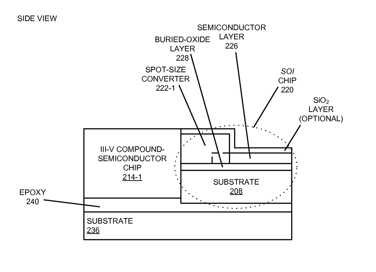
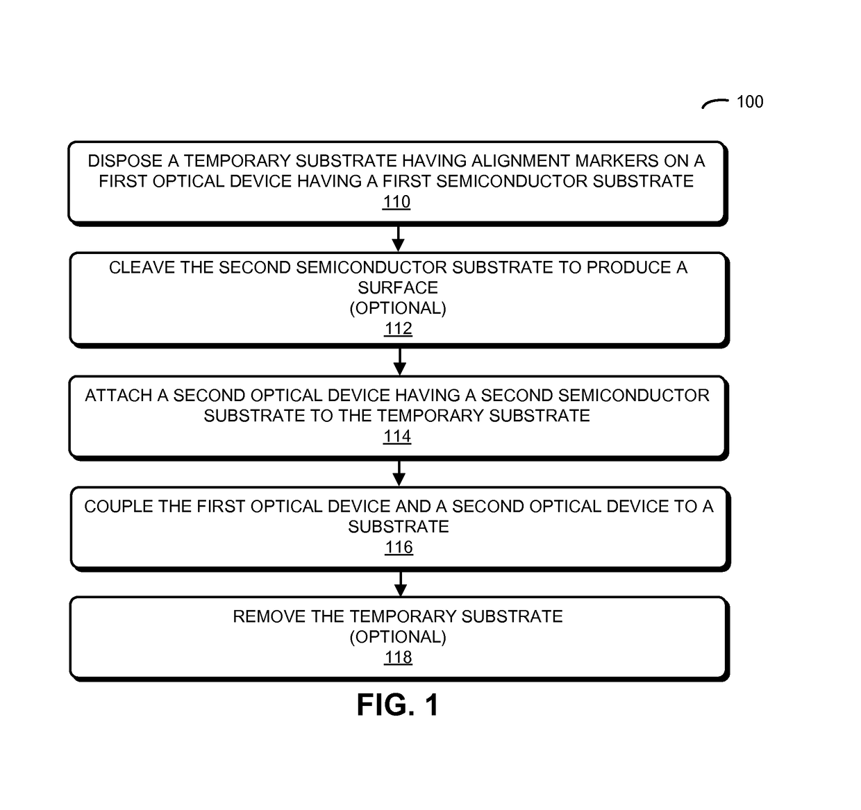
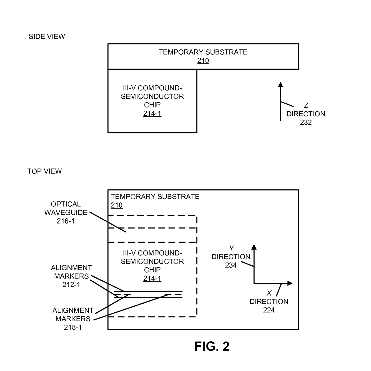
[0039]Embodiments of a co-planar hybrid optical source, a system that includes the hybrid optical source, and a method for fabricating the hybrid optical source are described. During this fabrication technique, a III-V compound-semiconductor active gain medium is integrated with a silicon-on-insulator (SOI) chip (or wafer) using edge coupling to form a co-planar hybrid optical source. Using a backside etching-assisted cleaving technique, and a temporary transparent substrate with alignment markers, a III-V compound-semiconductor chip with proper edge polish and coating can be integrated with a processed SOI chip (or wafer) with accurate alignment. This fabrication technique may significantly reduce the alignment complexity when fabricating the hybrid optical source, and may enable wafer-scale integration.

[0040]The fabrication technique may allow fabrication of a high-yield, low-cost and high-performance hybrid optical source. Consequently, the fabrication technique may enable the us...


PUM


Abstract

A technique for fabricating a hybrid optical source is described. During this fabrication technique, a III-V compound-semiconductor active gain medium is integrated with a silicon-on-insulator (SOI) chip (or wafer) using edge coupling to form a co-planar hybrid optical source. Using a backside etch-assisted cleaving technique, and a temporary transparent substrate with alignment markers, a III-V compound-semiconductor chip with proper edge polish and coating can be integrated with a processed SOI chip (or wafer) with accurate alignment. This fabrication technique may significantly reduce the alignment complexity when fabricating the hybrid optical source, and may enable wafer-scale integration.

Description

GOVERNMENT LICENSE RIGHTS[0001]This invention was made with Government support under Agreement No. HR0011-08-9-0001 awarded by DARPA. The Government has certain rights in the invention.BACKGROUND[0002]Field[0003]The present disclosure generally relates to the fabrication of a hybrid optical source. More specifically, the present disclosure relates to fabrication of a hybrid optical source with two co-planar, edge-coupled optical devices coupled to a substrate.[0004]Related Art[0005]Optical signaling based on silicon photonics has the potential to alleviate off-chip bandwidth bottlenecks, as well as to provide low latency intra-chip and chip-to-chip communication. Optical interconnects with these capabilities can facilitate new system architectures that include multiple chips, with multi-threaded cores. These optical interconnects can provide: high-bandwidth, low-latency and energy-efficient data communication.[0006]In the last few years, significant progress has been made in develop...

Claims


Application Information

Patent Timeline
Patent Type & Authority Patents(United States)
IPC IPC(8): G02B6/42G02B6/14
CPCG02B6/4224G02B6/14
Inventor ZHENG, XUEZHESHUBIN, IVANLUO, YINGLI, GUOLIANGKRISHNAMOORTHY, ASHOK V.
Owner ORACLE INT CORP
Learn More