

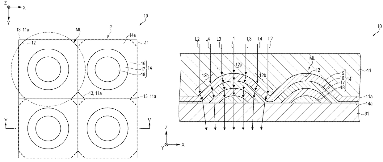
Lens array substrate, method of manufacturing lens array substrate, electro-optical device, and electronic apparatus
a technology of array substrate and lens, which is applied in the field of lens array substrate, can solve the problems of reduced contrast of liquid crystal devices and inability to easily adjust the optical path length, and achieve satisfactory contrast and bright display
- Summary
- Abstract
- Description
- Claims
- Application Information
AI Technical Summary
Benefits of technology
Problems solved by technology
Method used
Image

Examples
first embodiment
Electro-Optical Device
[0047]Here, a description will be given by taking an example of an active matrix type liquid crystal device, including a thin film transistor (TFT) as a switching element of a pixel, as an electro-optical device. For example, the liquid crystal device can be preferably used as a liquid crystal light valve of a projector to be described later.
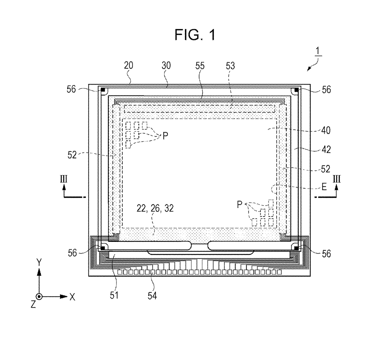
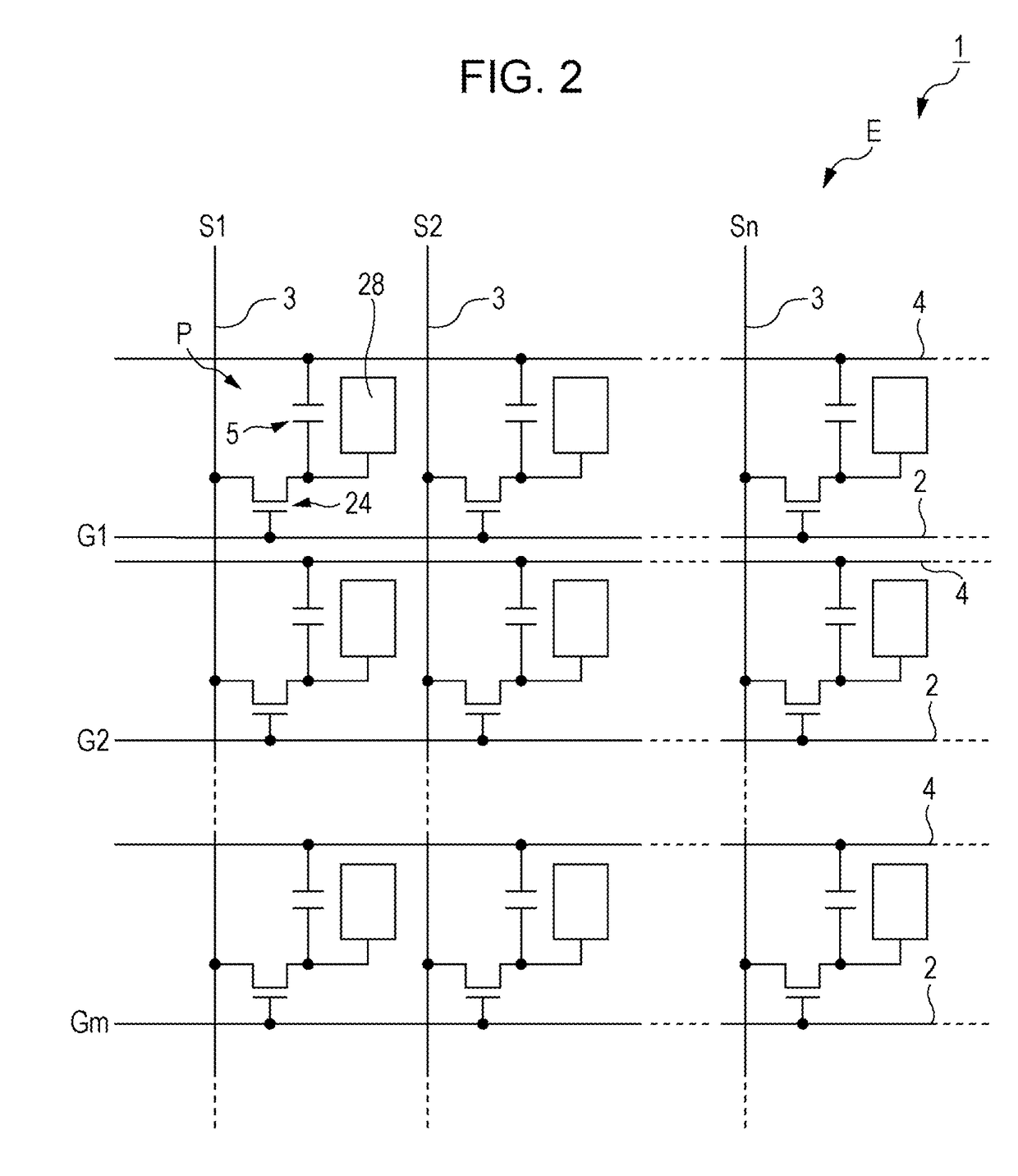
[0048]First, a liquid crystal device as an electro-optical device according to a first embodiment will be described with reference to FIGS. 1 to 3. FIG. 1 is a schematic plan view illustrating the configuration of the liquid crystal device according to the first embodiment. FIG. 2 is an equivalent circuit diagram illustrating an electrical configuration of the liquid crystal device according to the first embodiment. FIG. 3 is a schematic cross-sectional view illustrating the configuration of the liquid crystal device according to the first embodiment. In detail, FIG. 3 is a schematic cross-sectional view taken along line II...
second embodiment
Microlens Array Substrate
[0128]A microlens array substrate according to a second embodiment is different from that in the first embodiment in terms of the configuration of a lens layer. The configuration of a microlens array substrate 10A according to the second embodiment will be described below with reference to FIGS. 8 and 9. FIG. 8 is a schematic plan view illustrating the configuration of the microlens array substrate according to the second embodiment. FIG. 9 is a schematic cross-sectional view illustrating the configuration of the microlens array substrate according to the second embodiment. In detail, FIG. 9 is a schematic cross-sectional view taken along line IX-IX of FIG. 8. Components in common with those in the first embodiment are denoted by the same reference numerals, and the description thereof will be omitted here.
[0129]As illustrated in FIG. 9, the microlens array substrate 10A according to the second embodiment includes a substrate 11 provided with a concave porti...
third embodiment
Electronic Apparatus
[0140]Next, an electronic apparatus according to a third embodiment will be described with reference to FIG. 10. FIG. 10 is a schematic diagram illustrating the configuration of a projector as an electronic apparatus according to the third embodiment.
[0141]As illustrated in FIG. 10, a projector (projection type display device) 100 as an electronic apparatus according to the third embodiment includes a polarized illumination device 110, two dichroic mirrors 104 and 105, three reflecting mirrors 106, 107, and 108, five relay lenses 111, 112, 113, 114, and 115, three liquid crystal light valves 121, 122, and 123, a cross dichroic prism 116, and a projection lens 117.
[0142]The polarized illumination device 110 includes a lamp unit 101 as a light source constituted by a white light source such as, for example, an ultra-high pressure mercury lamp or a halogen lamp, an integrator lens 102, and a polarization conversion element 103. The lamp unit 101, the integrator lens...
PUM
| Property | Measurement | Unit |
|---|---|---|
| refractive index | aaaaa | aaaaa |
| contour shape | aaaaa | aaaaa |
| angle | aaaaa | aaaaa |
Abstract
Description
Claims
Application Information