Scanning 3D imager

a 3d imager and scanning technology, applied in the field of scanning 3d imagers, can solve the problems of difficult implementation, large disadvantage of high-power light requirements, and many measurement errors in the analog tof measurement technique, and achieve the effect of improving performan

Active Publication Date: 2017-04-11
IEE INT ELECTRONICS & ENG SA
View PDF10 Cites 42 Cited by
  • Summary
  • Abstract
  • Description
  • Claims
  • Application Information

AI Technical Summary

Benefits of technology

[0021]During operation, the 3D imager illuminates the scene slice after slice. As the scanning mirror oscillates about its tilting axis, the fan-shaped light beam is swept through the scene transversally (preferably perpendicularly) to the main direction of extension of the linear cross section of the light beam. The combination of the preferably essentially one-dimensional photosensor array and the scanning movement carried out by the moving mirror placed in the light path allows obtaining complete images of the scene, the images being 3D images in the sense that they have pixels disposed in rows and columns, each pixel comprising distance information.
[0022]The scan can be done at a low frequency, e.g. below 1 kHz. A reasonable frame repetition rate can even be obtained at 25 Hz, whereas more than 10 kHz were needed for a fully mechanical 2D scan. The scanning mirror can thus be relatively large, leading to good optical aperture and an easily controllable, well-defined, time function of the angular motion. Also, thanks to the lower scanning frequency, the time spans, during which the sensor points to specific slices of the scene is quite long. Together with the improved optical aperture, this leads to a longer distance range (i.e. the range from the smallest to the largest measurable distance) of this 3D imager, compared to the conventional 3D imagers. The 3D imager according to the invention thus may be implemented to achieve high resolution with a simple imager chip and a simple low-frequency oscillating mirror. The light source may be operated with reasonable pulse power at low repetition rate. With 1000 light pulses (or light flashes) per mirror sweep and 50 sweeps per second, the time span allows a distance range of more than 100 meters to be covered. Resolutions above VGA format, even HD, become feasible with a 1000-pixel photosensor line on the imager chip.
[0024]The evaluation circuitry is preferably arranged close to the photo-sensitive area of the photosensor, because sub-nanosecond reaction times are typically required to achieve the targeted accuracy in the distance measurement. The imager chip may be made using a standard silicon substrate. However, other substrates, e.g. silicon-germanium, may be used to implement very fast circuitry and thus to improve the performance of the imager.
[0025]Photosensors for very fast detection of individual photons are known, e.g. the so-called SPADs (single photon avalanche diodes). Photo-sensitivity of SPADs is high as single photons lead to a detectable discharge (countable and tagged with a time stamp) in the semiconductor. Optionally, individual micro-lenses on top of the semiconductor focus the light on the most sensitive area, which increases the effective optical fill factor.
[0027]One geometrical pixel of the imager chip can group plural individual photosensors in order to improve the production yield, the fill factor and even the dynamic light intensity range, while detected pulses may still be processed individually.

Problems solved by technology

This analog ToF measurement technique is subject to many measurement errors that require special measures to correct them.
Background light suppression is theoretically possible but proves to be difficult to implement.
This high power light requirement represents a major disadvantage for many applications.
The major disadvantage is the very high power of the IR light source.
Imaging features of such devices were typically limited to scanning one or two planes by using a rotating polygonal mirror.
LADAR instruments, which are mainly used in military applications and in scientific experiments, are traditionally expensive.
Imaging performance is poor and the time required for recording a complete image very long.
The power of the emitted laser light pulse is limited by cost and eye safety rules.
Larger mirrors have a mass versus stiffness conflict.
On the other hand, image quality needs a well-defined mirror surface shape; this means high stiffness, which requires a thick, i.e. heavy, mirror.
This means, in turn, that the scan time efficiency is low (below about 20%).
A mechanically stable mirror will thus be limited to a few millimeters in diameter, resulting in a poor optical aperture.
This technique has an obvious problem to achieve simultaneously high 2D resolution, high frame rate and a significant distance range.
This type of 3D imager is thus typically limited to a distance range of about 10 m and / or an image resolution of less than 10000 pixels.
Nevertheless, the major problem is to achieve high-resolution chips, because TDC and other circuitry limits the available photo-sensitive area.
Also, deep local storage structures for multiple event handling as well as data access busses are in conflict with optimal photon sensitivity and high image resolution.
Another problem of such a setup is the high power of the laser flash needed to illuminate the entire scene at once.
In general, today's bottleneck is not in computing power but in available real-time information for the computer.

Method used


Image

  • Scanning 3D imager
  • Scanning 3D imager
  • Scanning 3D imager

Examples


Embodiment Construction

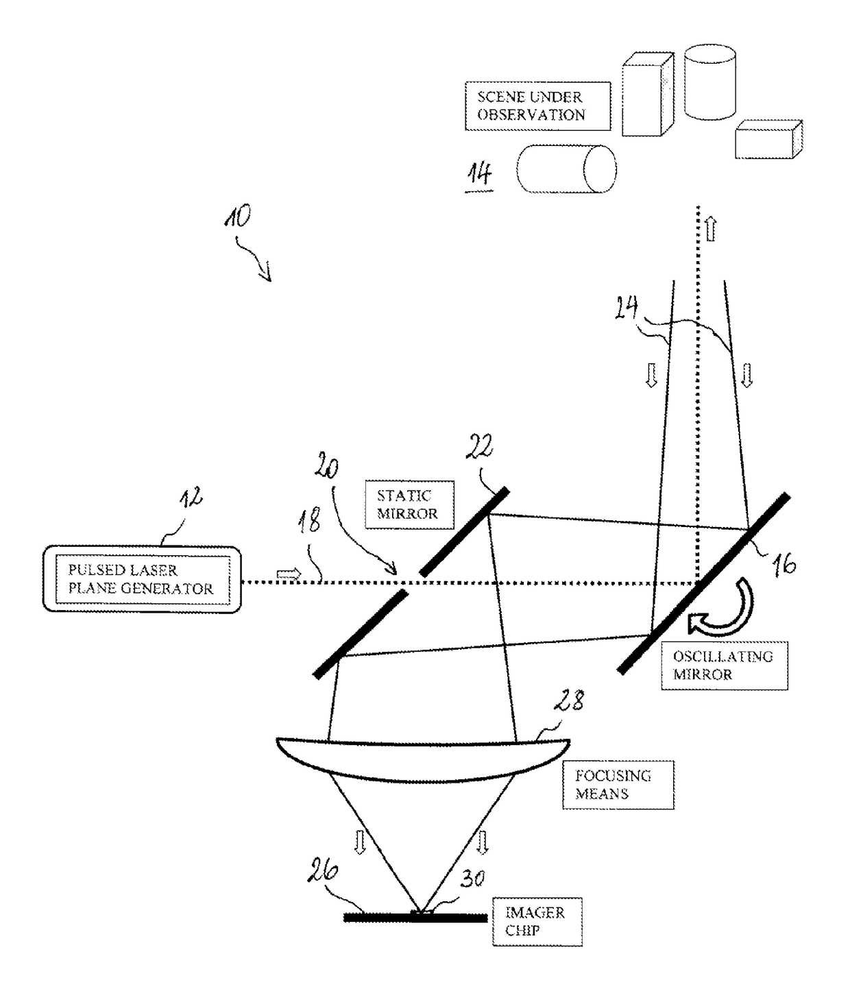
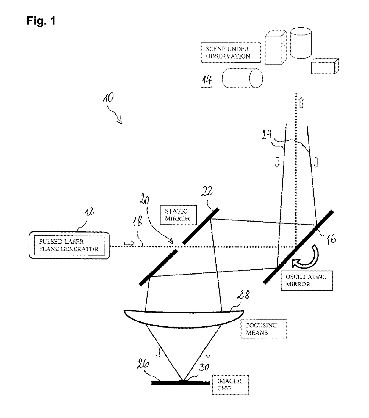
[0038]FIG. 1 shows a scanning 3D imager 10, comprising a pulsed laser source 12 as a light source. The pulsed laser beam is fanned out with a cylindrical lens (not shown) and directed into the scene 14 to be imaged by means of an oscillating scanning mirror 16 arranged in the light path of the laser beam 18. The laser beam thus successively illuminates slices of the scene 16 as it is swept through the scene transversally to the plane in which the laser beam has been fanned out. In FIG. 1, the laser beam 18 is fanned out perpendicular to the plane of the sheet. Between the pulsed laser source 12 and the oscillating mirror, the fan-shaped laser beam passes a slit 20 arranged in a static deflection mirror 22 arranged at 45°, which directs light that is scattered back 24 from the scene 14 onto an imager chip 26. A cylindrical focusing lens 28 focuses oriented in such a way that the illuminated slices of the scene are imaged thereon.

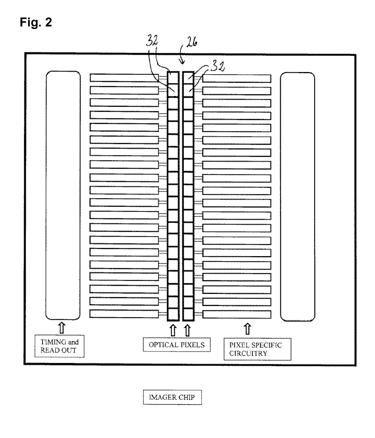
[0039]FIG. 2 schematically shows the imager chip 26 of ...


PUM


Abstract

A scanning 3D imager for recording images of a scene comprises a light source configured to emit a fan-shaped pulsed light beam with linear cross section, a scanning mirror arranged in the light path of the light beam to guide the light beam into the scene and to successively illuminate slices of the scene by sweeping the light beam through the scene transversally to the linear cross section thereof, and an imager chip arranged to receive light from the scene via the scanning mirror, the imager chip comprising an photosensor array disposed in such a way that the illuminated slices of the scene are successively imaged thereon.

Description

TECHNICAL FIELD[0001]The present invention relates to a scanning 3D imager, in particular such an imager that operates according to the time-of-flight (ToF) measurement principle.BRIEF DESCRIPTION OF RELATED ART[0002]Systems for creating a three-dimensional (3D) representation of a given portion of space have a variety of potential applications in many different fields. Examples are automotive sensor technology (e.g. vehicle occupant detection and / or classification), automation technology, or surveillance technology (e.g. plant monitoring, people counting, access control and pedestrian detection), to name only a few.[0003]According to the ToF distance measurement principle, a light signal is emitted into the scene of interest and the time between the emission and the echo-return of the emitted signal is measured. The corresponding distance is proportional to the measured time-of-flight. For the purposes of the present description, the term “light” is to be understood as including vi...

Claims


Application Information

Patent Timeline
Patent Type & Authority Patents(United States)
IPC IPC(8): H04N13/02H04N1/03G01S17/89G01S7/481G01S7/486G02B26/10G01S7/4863
CPCH04N13/0253G01S17/89G01S7/4817G01S7/4863G02B26/105H04N13/254
Inventor FEDERSPIEL, LAURENT
Owner IEE INT ELECTRONICS & ENG SA
Why Eureka
Try Eureka