High density programmable e-fuse co-integrated with vertical FETs

a programmable e-fuse and high density technology, applied in the direction of semiconductor devices, semiconductor/solid-state device details, diodes, etc., can solve the problem that e-fuses can consume valuable chip spa

Inactive Publication Date: 2017-08-08
ELPIS TECH INC
View PDF9 Cites 35 Cited by
  • Summary
  • Abstract
  • Description
  • Claims
  • Application Information

AI Technical Summary

Problems solved by technology

Despite their usefulness, e-fuses can consume valuable chip space.

Method used


Image

  • High density programmable e-fuse co-integrated with vertical FETs
  • High density programmable e-fuse co-integrated with vertical FETs
  • High density programmable e-fuse co-integrated with vertical FETs

Examples


Embodiment Construction

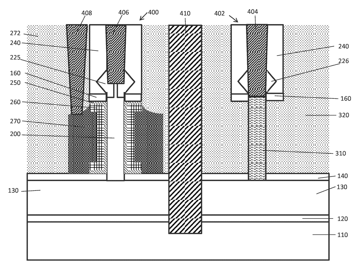
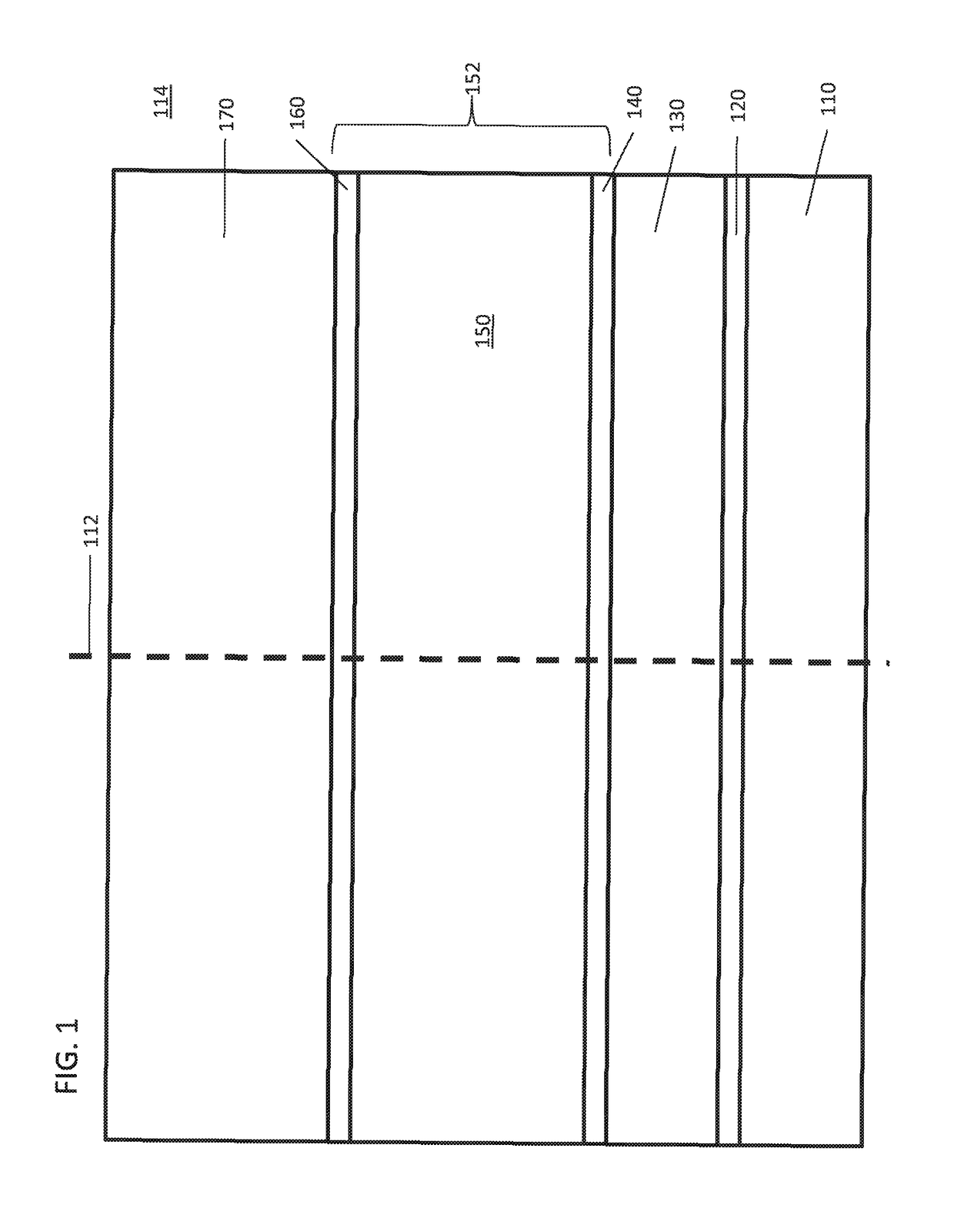
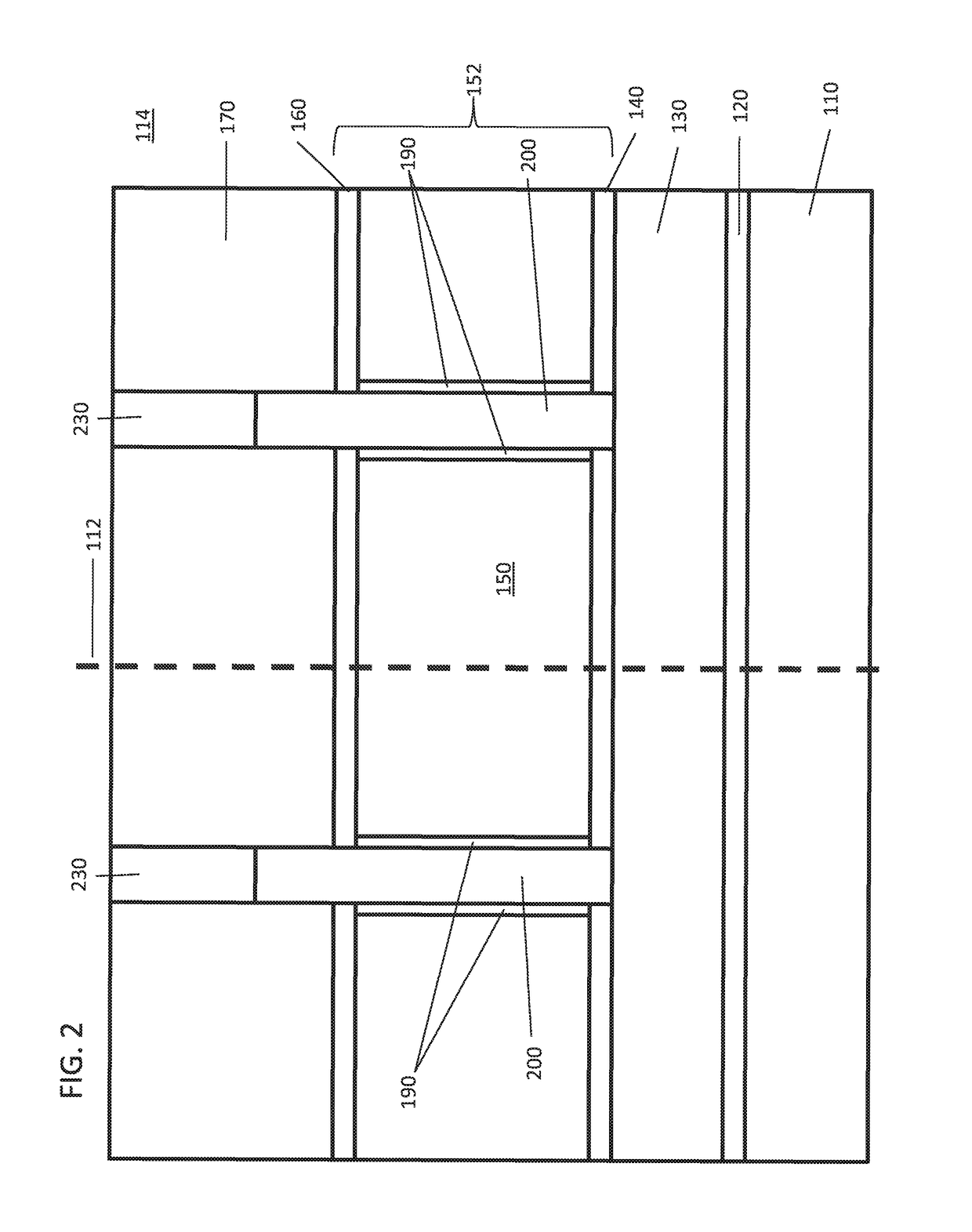
[0020]In accordance with the present principles, co-integration of programmable electrical-fuse (e-fuse) devices with vertical field effect transistors (FET) is provided. Vertical transistors provide an option for scaling of node sizes (e.g., for 5 nm technology and beyond). A channel-last replacement metal-gate gate all-around vertical transistor programmable e-fuse device is obtained by siliciding inside a channel trench and then contacting a cathode (bottom) and anode (top). A narrow channel serves as a fuse link, whose length can be equivalent to a channel length of any fabricated vertical transistors.

[0021]The channel-last fabrication approach forms vertical field effect transistors (VFETs), or more specifically, vertical finFETs, where current flows vertically through the channel, and vertical e-fuses on the same substrate. The vertical finFETs and vertical e-fuses may be epitaxially grown on a coterminous region of a substrate surface implementing various fabrication processe...


PUM


Abstract

A method for integrating vertical transistors and electric fuses includes forming fins through a dielectric layer and a dummy gate stack on a substrate; thinning top portions of the fins by an etch process; epitaxially growing top source / drain regions on thinned portions of the fins in a transistor region and top cathode / anode regions on the thinned portions of the fins in a fuse region; and removing the dummy gate layer and exposing sidewalls of the fins. The fuse region is blocked to form a gate structure in the transistor region. The transistor region is blocked and the fuse region is exposed to conformally deposit a metal on exposed sidewalls of the fins. The metal is annealed to form silicided fins. Portions of the substrate are separated to form bottom source / drain regions for vertical transistors in the transistor region and bottom cathode / anode regions for fuses in the fuse region.

Description

BACKGROUND[0001]Technical Field[0002]The present invention generally relates to semiconductor processing and devices, and more particularly, to electrical fuses (e-fuses) disposed vertically and co-integrated with field effect transistors (FETs).[0003]Description of the Related Art[0004]Programmable electrical fuses (e-fuses) provide a plurality of functions on semiconductor devices. These functions may include uses for applications such as memory array redundancy, post-manufacture programming of circuits, and package identification coding. Despite their usefulness, e-fuses can consume valuable chip space.SUMMARY[0005]In accordance with an embodiment of the present principles, a method for integrating vertical transistor and vertical electric fuses includes forming fins through a dielectric layer and a dummy gate stack on a substrate, the dummy gate stack including a bottom spacer, a dummy gate layer and a top spacer layer; thinning top portions of the fins by an etch process; epita...

Claims


Application Information

Patent Timeline
Patent Type & Authority Patents(United States)
IPC IPC(8): H01L23/525H01L27/112H01L21/762H01L21/768H01L23/535H01L29/423H01L29/786H01L29/66H01L29/06H01L27/06
CPCH01L27/11206H01L29/42392H01L29/78642H01L29/78696H01L29/66666H01L29/66545H01L29/0653H01L23/5256H01L23/535H01L21/76805H01L21/76895H01L21/76224H01L27/0629H01L21/84H01L29/66742H10B20/20
Inventor BALAKRISHNAN, KARTHIKGUILLORN, MICHAEL A.HASHEMI, POUYAREZNICEK, ALEXANDER
Owner ELPIS TECH INC
Why Eureka
Try Eureka