

Power MOSFET having planar channel, vertical current path, and top drain electrode
a power mosfet and planar channel technology, applied in the field of transistors, can solve the problems of reducing on-resistance, reducing breakdown voltage, and affecting the performance of the circuit, and achieve the effect of improving the breakdown voltag
- Summary
- Abstract
- Description
- Claims
- Application Information
AI Technical Summary
Benefits of technology
Problems solved by technology
Method used
Image

Examples
Embodiment Construction
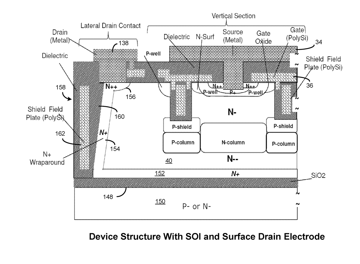
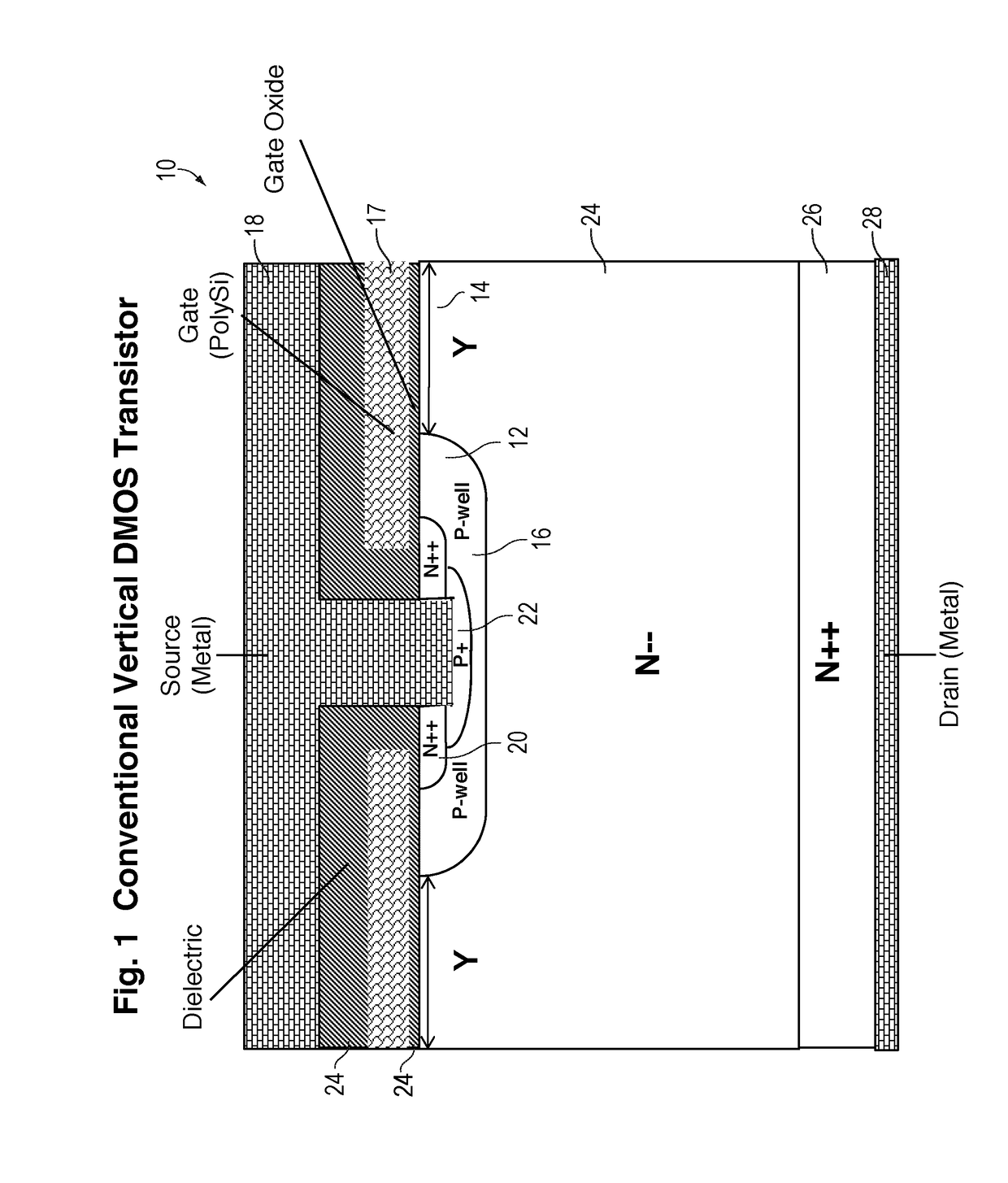
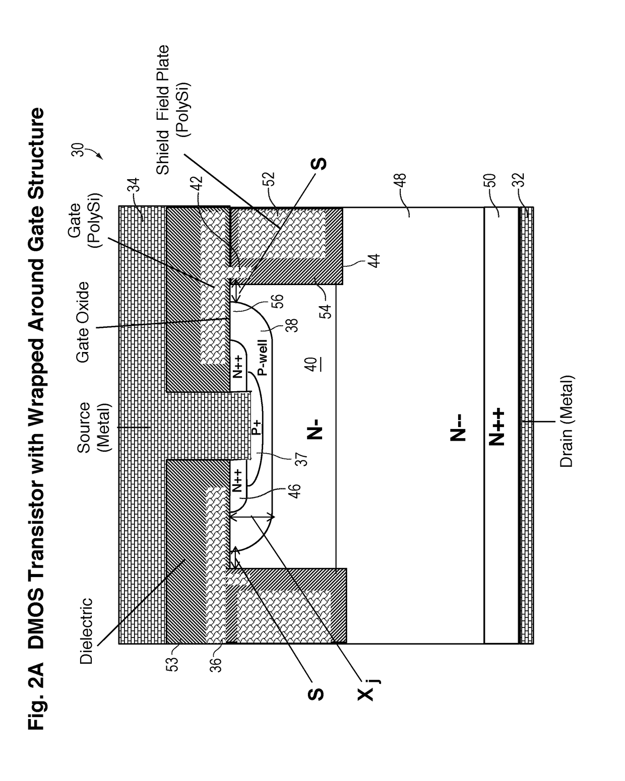
[0062]FIG. 2A is a cross-sectional view of a single vertical MOSFET cell 30 in an array of identical contiguous MOSFET cells connected in parallel in accordance with one embodiment of the invention. FIGS. 8A-8C, described later, illustrate various configurations of the cells, which include strips and closed cells. In the cross-sectional views, the various regions are not drawn to scale for ease of illustration. The simulation diagrams of FIGS. 7A and 7B show more accurate relative dimensions.
[0063]In FIG. 2A, the width of the cell 30 shown is about 5-15 microns. The cell 30 may have a breakdown voltage exceeding 600 volts, and the number of cells 30 in an array of identical cells determines the current handling ability, such as 20 Amps. The array of cells may be in strips, squares, hexagons, or other known shapes.
[0064]In one typical application, a load is connected between the bottom drain electrode 32 and a positive voltage supply, and the top source electrode 34 is connected to g...
PUM
 Abstract
Description
Claims
Application Information