Sub-threshold enabled flash memory system

a flash memory system and sub-threshold technology, applied in static storage, digital storage, instruments, etc., can solve the problems of unacceptable power consumption in sleep or standby mode, unacceptable time required to turn on the circuit, unacceptable long time required to begin normal memory read/write operations, etc., to avoid unnecessary proliferation of numbers

Active Publication Date: 2017-10-03
AMBIQ MICRO
View PDF26 Cites 1 Cited by
  • Summary
  • Abstract
  • Description
  • Claims
  • Application Information

AI Technical Summary

Benefits of technology

[0036]In the drawings, similar elements will be similarly numbered whenever possible. However, this practice is simply for convenience of reference and to avoid u

Problems solved by technology

Furthermore, it is of no relevance in such systems which specific voltage levels are selected to represent each of the logic states.
Unfortunately, the current consumed by these circuits often results in unacceptable power c

Method used


Image

  • Sub-threshold enabled flash memory system
  • Sub-threshold enabled flash memory system
  • Sub-threshold enabled flash memory system

Examples


Embodiment Construction

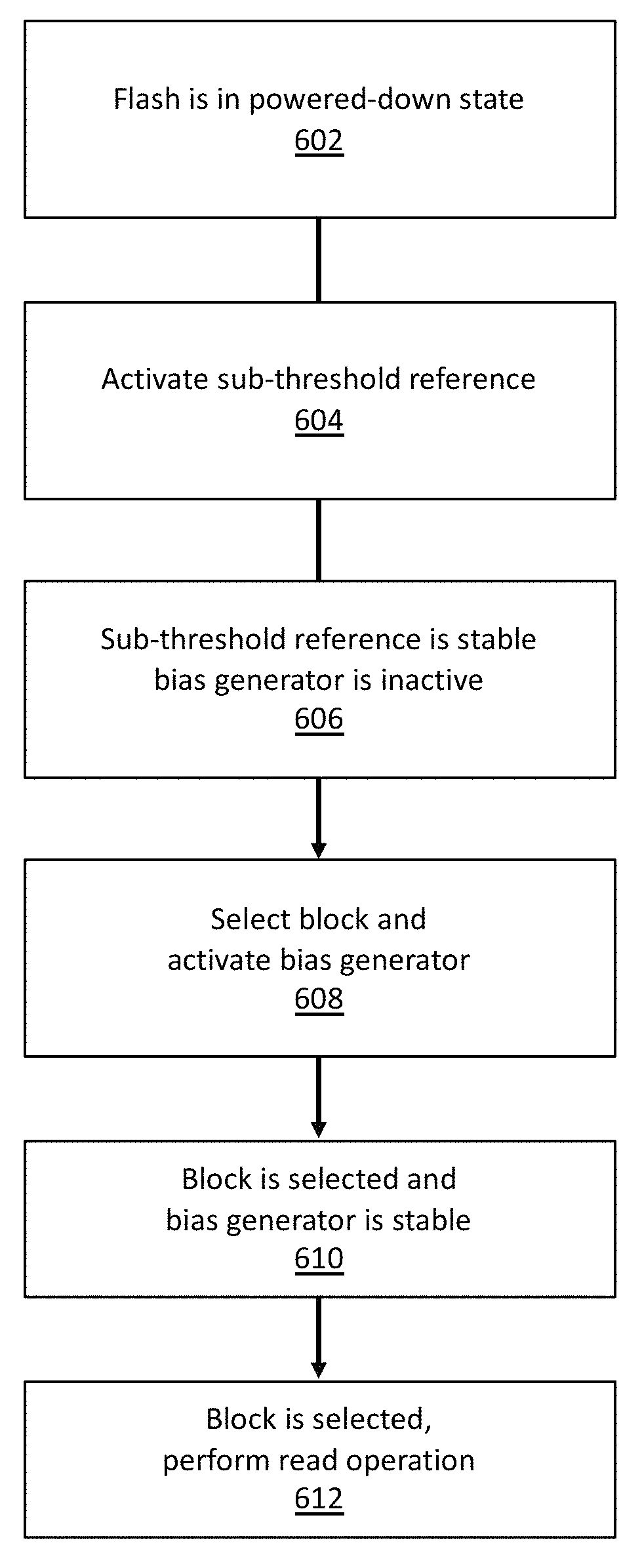
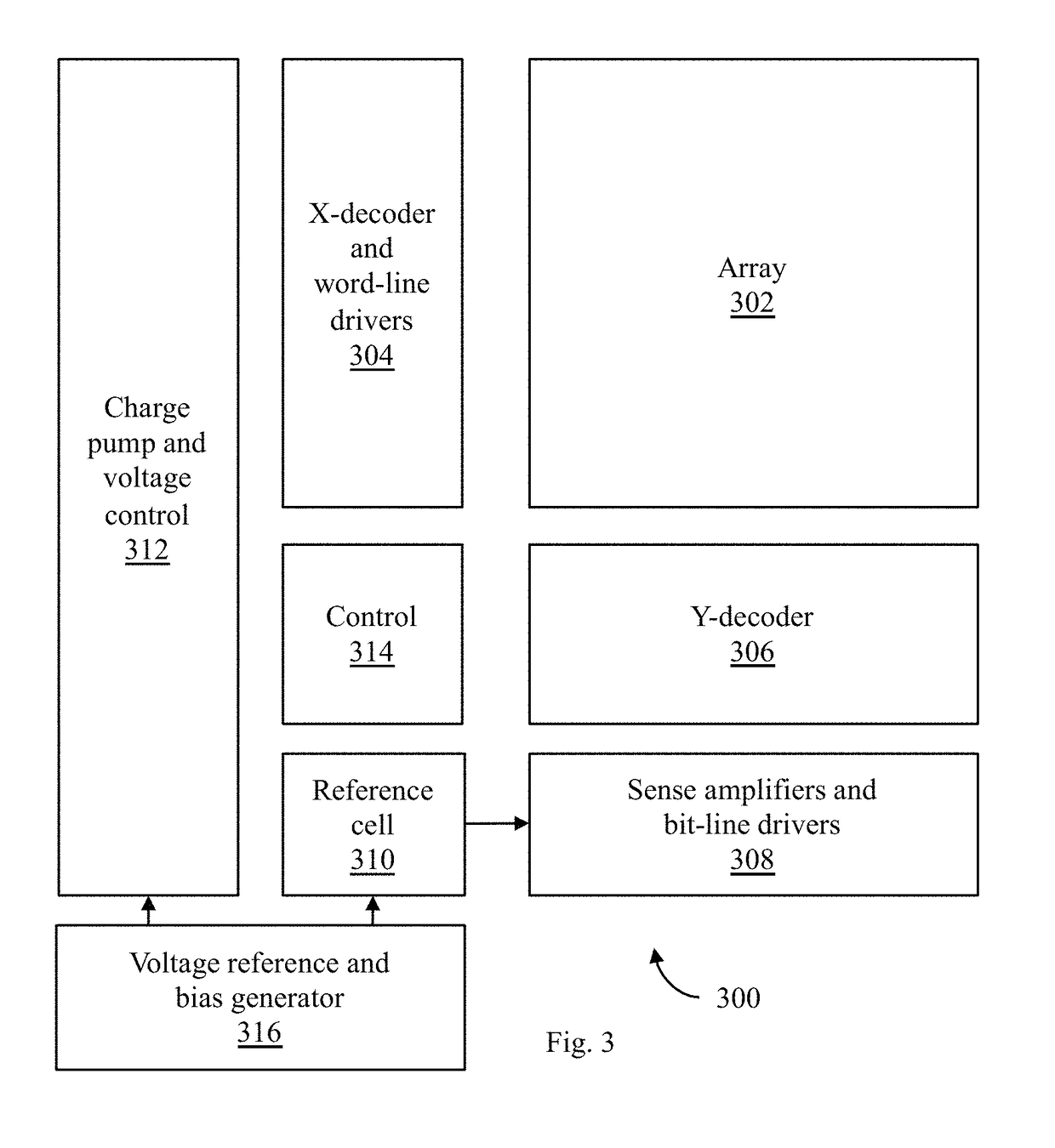
[0037]FIG. 3 schematically illustrates a block diagram of one embodiment of a non-volatile, charge-based flash memory system 300. The memory system 18 can be formed on a stand-alone flash die, or embedded with other circuits, including processors, microcontrollers, logic controllers, or sensor facilities with memory sub-systems. The memory system 300 includes a memory array 302 and supporting circuitry such as X-decoder and word-line drivers 304, Y-decoder 306, sense amplifiers and bit-line drivers 308, and a reference cell 310 that provides for charge comparison. Power to the array is provided by a charge pump and voltage control module 312, and overall control module 314 coordinates various required read, write, and power state switching activities of the memory system 300.

[0038]In accordance with one embodiment of the invention, both the charge pump and voltage control 312 and the reference cell 310 are connected to a voltage reference and bias generation facility 316. In the dis...


PUM


Abstract

A flash memory system for use in an electronic system comprising an integrated circuit such as a microcontroller. The flash memory system embodies one or more circuits adapted to operate at sub- or near-threshold voltage levels. These low-power circuits are selectively activated or de-activated to balance power dissipation with the response time of the memory system required in particular applications.

Description

CROSS-REFERENCE TO RELATED APPLICATIONS[0001]This application is related to the following:[0002]1. Provisional Application Ser. No. 62 / 066,218, filed 20 Oct. 2014 (“Parent Provisional”);[0003]2. PCT Application No. PCT / US15 / 50239, filed 15 Sep. 2015 (“Related Application 1”);[0004]3. U.S. application Ser. No. 14 / 855,105, filed 15 Sep. 2015 (“Related Application 2”); and[0005]4. U.S. application Ser. No. 14 / 918,384, filed 20 Oct. 2015 (“Related Application 3”).[0006]This application claims priority to the Parent Provisional, and hereby claims benefit of the filing date thereof pursuant to 37 CFR §1.78(a)(4).[0007]The subject matter of the Parent Provisional and all of the Related Applications, each in its entirety, is expressly incorporated herein by reference.BACKGROUND OF THE INVENTION[0008]1. Field of the Invention[0009]Non-volatile semiconductor memory systems having multiple power states are described. More specifically, components and methods for improving utilization and reduc...

Claims


Application Information

Patent Timeline
IPC IPC(8): G11C16/10G11C7/14
CPCG11C16/10G11C7/14G11C5/148G11C16/30
Inventor CHEVALLIER, CHRISTOPHE J.CERMAK, DANIEL M.HANSON, SCOTT
Owner AMBIQ MICRO
Why Eureka
Try Eureka