Structural member for electronic devices

a technology of structural members and electronic devices, applied in the field of structural members for electronic devices, can solve the problems of reducing the restoration properties, peeling between the members, and affecting the normal operation of the structure, and achieves the effects of high stress relaxation properties, excellent stress relaxation properties, and significant deformation

Active Publication Date: 2017-10-31
PANASONIC INTELLECTUAL PROPERTY MANAGEMENT CO LTD
View PDF47 Cites 6 Cited by
  • Summary
  • Abstract
  • Description
  • Claims
  • Application Information

AI Technical Summary

Benefits of technology

[0012]On the other hand, as properties required of a recent resin material in addition to flexibility, there are stress relaxation properties. High residual stress when stress is added and deformation occurs means that an amount of force required to recover its original shape is high. Therefore, when residual stress is high, peeling between members and breaking may occur. Therefore, to reduce added stress in order to reduce residual stress, that is, excellent stress relaxation properties are also necessary properties.
[0014]Therefore, a display manufactured by using such a resin has a problem in that peeling or breaking easily occurs due to residual stress when it follows a free-form surface or significantly deforms. Therefore, the flexible display remains in a state of having flexibility to a slight degree.
[0018]Here, the inventors extensively studied, and as a result, thought that by allowing high stress relaxation properties during tension and excellent restoration properties after extension, which are conflicting properties, to be compatible with each other, flexibility and restoration even after deformation can be achieved and peeling between members or breaking due to residual stress can be minimized. The inventors repeated examinations on the basis of the findings and completed the present invention.
[0019]That is, an aspect of the present invention is a structural member for electronic devices, which uses a resin composition that is elastically deformable and has low residual strain ratio and stress relaxation properties.
[0032]According to the present invention, it is thought that since high stress relaxation properties during tension and excellent restoration properties after extension are compatible with each other, it is possible to provide a structural member for electronic devices which uses the material that is flexible and has excellent stress relaxation properties. In addition, it is possible to provide a flexible display or the like which can follow a free-form surface or can cope with significant deformation by using the structure.
[0033]In addition, since the compatibility between high stress relaxation properties and restoration properties is provided, the structure can be applied to, in addition to the flexible display, various technology fields such as optical fields, electronic fields, adhesion fields, and medical fields and is thus very advantageous in industrial applications.

Problems solved by technology

High residual stress when stress is added and deformation occurs means that an amount of force required to recover its original shape is high.
Therefore, when residual stress is high, peeling between members and breaking may occur.
However, in this case, the restoration properties may be reduced.
In addition, there is also a problem in that the urethane resin has a narrow usable temperature range and low heat resistance, resulting in a limitation on the range of use.
Therefore, a display manufactured by using such a resin has a problem in that peeling or breaking easily occurs due to residual stress when it follows a free-form surface or significantly deforms.
These problems are similarly applied to other rubber materials, which means that the rubber materials have low stress relaxation properties while having high restoration properties.
Therefore, there is a problem in that the material cannot recover its original shape after extension (has high residual strain ratio) although it has excellent stress relaxation properties.

Method used


Image

  • Structural member for electronic devices
  • Structural member for electronic devices
  • Structural member for electronic devices

Examples


example 1

[Example 1] Structural Member for Electronic Devices in which Silicon Chip is Mounted

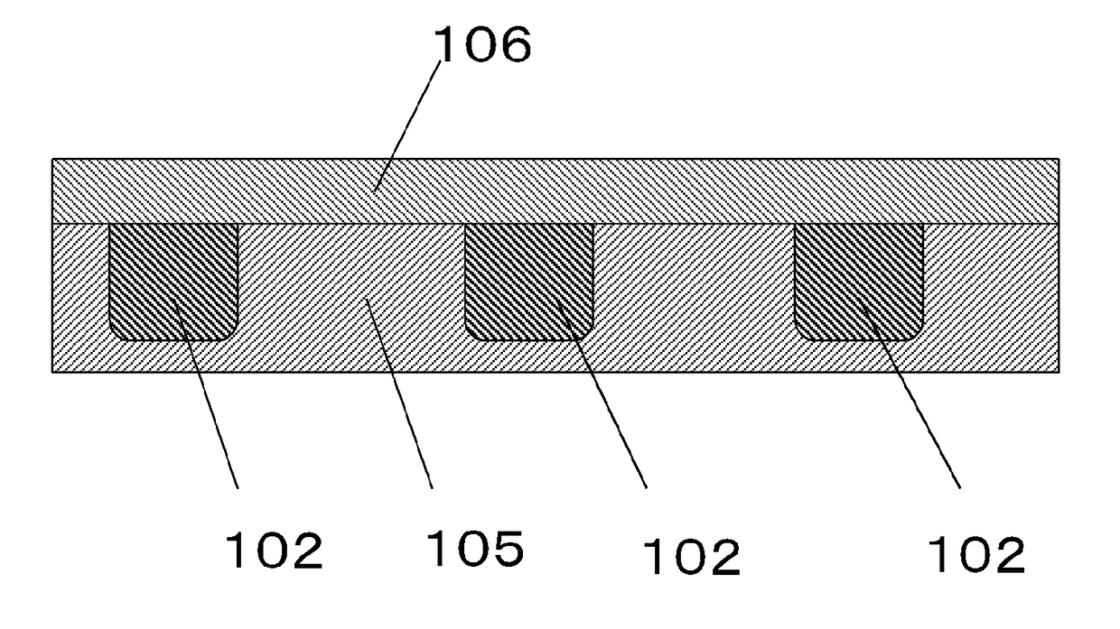
[0177]A structural member for electronic devices described in Example 1 is, as illustrated in FIG. 3, a structure in which a silicon chip that is electronic element 102 is mounted on sheet 101. Sheet 101 is made of a resin composition described in (Example 1-1) or (Example 1-2).

example 1-1

[0178]Sheet 101 in a semi-cured state was produced by applying resin composition 1 prepared as described above to a PET film and heating the resultant at 100° C. for 10 minutes. A silicon chip was attached thereto on a hot plate at 100° C., and the resultant was further heated and cured at 170° C. for 1 hour, thereby obtaining a sheet-like structure in which the silicon chip was mounted on sheet 101.

example 1-2

[0179]Resin composition 2 prepared as described above was prepared in the same manner as in (Example 1-1), thereby obtaining a sheet-like structure in which the silicon chip was mounted on sheet 101.


PUM

PropertyMeasurementUnit
lengthaaaaaaaaaa
widthaaaaaaaaaa
thicknessaaaaaaaaaa

Abstract

Provided is a structural member for electronic devices which uses a material that is flexible and has excellent restoration properties after extension and stress relaxation properties. The structural member for electronic devices has the following properties A and B: (Property A) In a case where predetermined deformation is applied, stress that applies the deformation is relaxed (reduced) with time: and (Property B) In a case where the stress that applies deformation is 0, the deformation rarely remains while a resin composition is recovered. That is, when stress is 0, residual strain substantially becomes 0 (specifically 3% or lower).

Description

BACKGROUND OF THE INVENTION[0001]1. Field of the Invention[0002]The present invention relates to a structural member for electronic devices, which uses a resin composition having high tensile stress relaxation properties and excellent restoration properties after extension.[0003]2. Description of the Related Art[0004]A thermosetting resin has been used in a wide range of fields such as electronic materials and optical materials due to its excellent heat resistance, chemical resistance, moldability, insulation reliability, and the like. Particularly, as the thermosetting resin, an epoxy resin is widely used for various purposes. However, it is also known that the epoxy resin is generally hard and has insufficient flexibility although the above-mentioned properties are excellent. Therefore, the epoxy resin may be deformed or broken due to stress or heat stress from the outside.[0005]As a material having more excellent flexibility, there are thermoplastic resins such as polyethylene or...

Claims


Application Information

Patent Timeline
Patent Type & Authority Patents(United States)
IPC IPC(8): B32B27/36B32B27/38C08L71/02B32B3/08C08G59/24C08L63/00C08L3/02C08G59/56B32B3/30B32B27/20B32B7/04B32B27/08
CPCB32B27/36B32B27/38C08G59/245C08G59/56C08L63/00C08L71/02C08L87/00B32B2571/00B32B3/08B32B3/30B32B7/045B32B27/08B32B27/20B32B2305/77B32B2307/202B32B2307/21B32B2307/50B32B2307/51B32B2307/546B32B2307/552B32B2307/734B32B2457/00B32B2457/20B32B7/05
Inventor ABE, TAKATOSHISAWADA, TOMOAKIYOSHIOKA, SHINGO
Owner PANASONIC INTELLECTUAL PROPERTY MANAGEMENT CO LTD
Why Eureka
Try Eureka