Compound semiconductor photonic integrated circuit with dielectric waveguide

a dielectric waveguide and semiconductor technology, applied in multiplex communication, instruments, optical elements, etc., can solve the problems of poor design methodologies, low manufacturing yield, cost barriers, etc., and achieve the effect of reducing power losses, reducing the effect of thin film interference, and reducing the variation of refractive index with temperatur

Active Publication Date: 2018-01-30
POET TECH
View PDF30 Cites 16 Cited by
  • Summary
  • Abstract
  • Description
  • Claims
  • Application Information

AI Technical Summary

Benefits of technology

[0017]The dielectric waveguide is composed of materials that have a lower variation of refractive index with temperature. To reduce power losses, the dielectric waveguide is mode matched to the waveguide of the PIC. The PIC further includes an anti-reflection coating layer deposited between the waveguide and the dielectric waveguide to reduce the effect of thin film interference. As no heater and thermoelectric coolers are involved in temperature control, the overall size of the PIC is reduced.

Problems solved by technology

However, even such monolithic integration can provide cost barriers with poor design methodologies, low manufacturing yields, complicated manufacturing processes, and repeated expensive epitaxial growth processes.
However, as we move from considering a single DFB laser through to a 4-channel, 16-channel, and a 40-channel PIC, such as CWDM and DWDM receivers with integrated photodiodes, the die footprint increases significantly, primarily from the WDM component, such that active temperature stabilization becomes increasingly difficult to achieve.
Further, there are additional issues that arise with integration, for example, thermal crosstalk between adjacent elements and the like.
However, heaters and thermo-electric coolers can require significant electrical power consumption and also impose complex thermal management requirements upon the die packaging even for just a passive DWDM to ensure uniform temperature even before active devices are considered.
Furthermore, when an InP waveguide is deposited on an SiO2 substrate, due to mismatch between the lattice structure of the InP waveguide and the SiO2, the InP waveguide cracks due to high stress between the InP waveguide and the SiO2 substrate.

Method used


Image

  • Compound semiconductor photonic integrated circuit with dielectric waveguide
  • Compound semiconductor photonic integrated circuit with dielectric waveguide
  • Compound semiconductor photonic integrated circuit with dielectric waveguide

Examples


Embodiment Construction

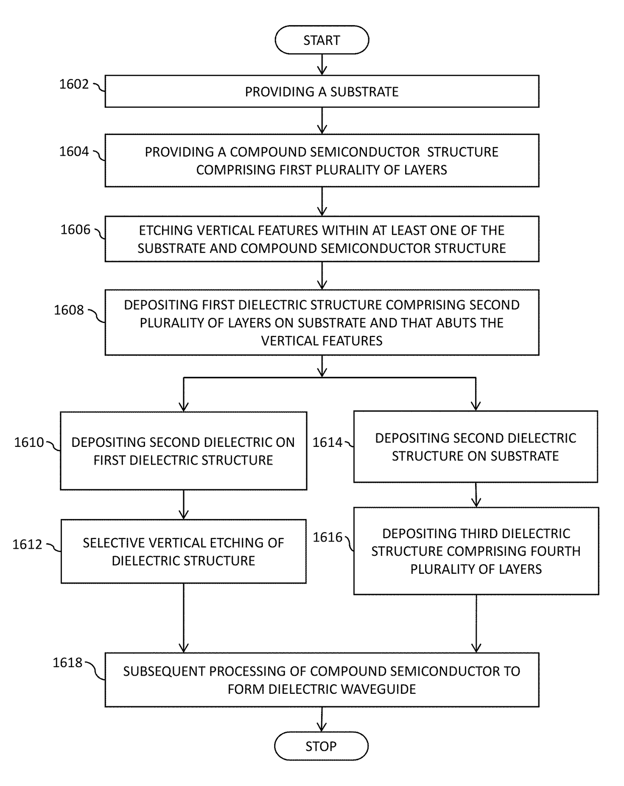
[0042]The present invention is directed to photonic integrated circuits and more particularly to dielectric waveguides and dielectric structures on semiconductor substrates and photonic circuits.

[0043]The ensuing description provides exemplary embodiment(s) only, and is not intended to limit the scope, applicability or configuration of the disclosure. Rather, the ensuing description of the exemplary embodiment(s) will provide those skilled in the art with an enabling description for implementing an exemplary embodiment. It being understood that various changes may be made in the function and arrangement of elements without departing from the spirit and scope as set forth in the appended claims.

[0044]An “emitter” or “distributed feedback (DFB) laser” or “light emitting diode” (LED) as used herein and throughout this disclosure refers to, but is not limited to, a type of optical emitter that uses semiconductor light emitting structures such as semiconductor junctions, pn junctions, pi...


PUM


Abstract

A photonic integrated circuit (PIC) is grown by epitaxy on a substrate. The PIC includes at least one active element, at least one passive element, and a dielectric waveguide. The at least one active and passive elements are formed over the substrate and are in optical contact with each other. The dielectric waveguide is formed over the substrate, and is in optical contact with the at least one active and passive elements. The at least one active and passive elements each are formed using a III-V compound semiconductor material.

Description

FIELD OF THE INVENTION[0001]This invention relates to photonic integrated circuits and more particularly to dielectric waveguides and dielectric structures on semiconductor substrates and photonic integrated circuits.BACKGROUND OF THE INVENTION[0002]Photonic Integrated Circuits (PICs) integrate different optical functionalities on a single photonic chip. The PICs enable the production of complex optical circuits using high volume semiconductor wafer fabrication techniques. Due to the above mentioned abilities, the PICs are utilized in optical communication networks. Accordingly, they offer to reduce component footprint, eliminate multiple packaging issues and multiple optical alignments, and eventually achieve the unprecedented cost efficiency and volume scalability in mass production of consumer photonics products.[0003]In the context of applications, the advantages of PIC become especially compelling when active waveguide devices such as laser, photodetector, and the like, are com...

Claims


Application Information

Patent Timeline
Patent Type & Authority Patents(United States)
IPC IPC(8): G02B6/12H04B10/00G02B6/124G02B6/136G02B6/122G02B6/13G02B6/132
CPCG02B6/12004G02B6/124G02B6/12016G02B6/1228G02B6/131G02B6/136H04B10/00G02B6/132G02B2006/12157G02B2006/12104G02B2006/12135H04J14/0208
Inventor FLORJANCZYK, MIROSLAWRING, WILLIAM
Owner POET TECH
Why Eureka
Try Eureka