
Resin composition, resin film, and semiconductor device and method for manufacturing same

a resin film and semiconductor technology, applied in the direction of synthetic resin layered products, coatings, chemistry apparatus and processes, etc., can solve the problems of difficult to optimize the flow and physical properties of liquid, difficult to precisely control the molding range of compression molding techniques at the end portion of the wafer, wire deformation, etc., to achieve satisfactory encapsulation or molding performance, improve adhesion, and reduce warpage

Active Publication Date: 2018-02-13
SHIN ETSU CHEM IND CO LTD
View PDF14 Cites 0 Cited by
  • Summary
  • Abstract
  • Description
  • Claims
  • Application Information

AI Technical Summary

Benefits of technology

The invention is a resin composition that can be made into a film for encapsulating or molding wafers. The resin film has good adhesion, low warping and provides protection to the wafer. This resin composition can be used in wafer-level packaging and is useful for manufacturing semiconductor devices on a large scale. The resin composition is made of a silicone resin, an epoxy resin curing agent, and a filler. The combination of these components results in an effective material for encapsulating wafers, providing adhesion and protection to the wafer.

Problems solved by technology

However, the transfer molding technique can cause wire deformation because the resin is flowed into narrow gaps.
The compression molding technique is difficult to precisely control the molding range at an end portion of the wafer.
Also, it is not easy to optimize the flow and physical properties of the liquid encapsulating resin when it is fed into the molding machine.
With the recent transition of wafers toward larger diameter and reduced thickness, the warpage of the wafer after encapsulation, which is not noticeable in the prior art, becomes a problem.

Method used


Image

  • Resin composition, resin film, and semiconductor device and method for manufacturing same
  • Resin composition, resin film, and semiconductor device and method for manufacturing same
  • Resin composition, resin film, and semiconductor device and method for manufacturing same

Examples


examples

[0078]Synthesis Examples, Examples and Comparative Examples are given below by way of illustration and not by way of limitation.

synthesis examples 1 to 3

[0079]In Synthesis Examples, the weight average molecular weight (Mw) of a polymer was measured by gel permeation chromatography (GPC) versus monodisperse polystyrene standards, using GPC column TSKgel Super HZM-H (Tosoh Corp.) under conditions including tetrahydrofuran eluent, flow rate 0.6 mL / min and column temperature 40° C.

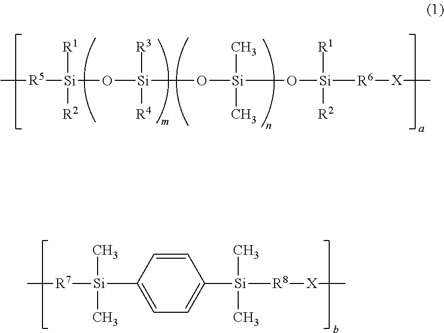
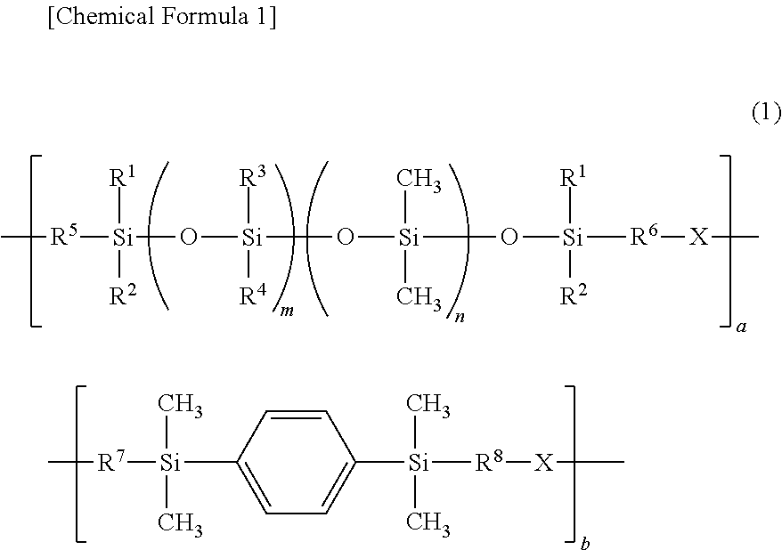
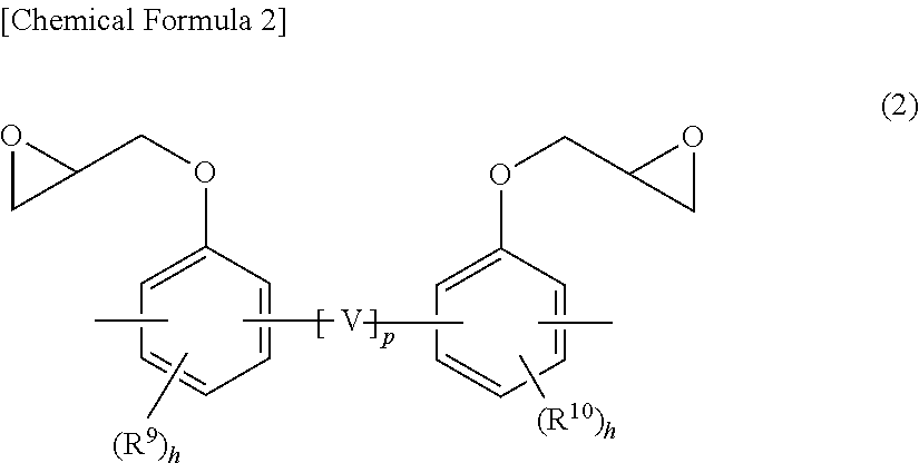
[0080]The compounds used in Examples and Comparative Examples are identified below.

[0081]

synthesis example 1

[0082]A 3-L flask equipped with a stirrer, thermometer, nitrogen purging line and reflux condenser was charged with 147 g (0.35 mol) of Compound S-1 and 27.9 g (0.15 mol) of Compound S-2, to which 2,000 g of toluene was added. The flask was heated at 70° C., after which 1.0 g of a toluene solution of chloroplatinic acid (Pt concentration 0.5 wt %) was admitted, and 77.8 g (0.4 mol) of Compound S-3 and 309.4 g (0.1 mol) of Compound S-4 wherein x=40 were added dropwise over 1 hour. This resulted in a ratio of (total moles of hydrosilyl groups) / (total moles of alkenyl groups) =1 / 1. At the end of dropwise addition, the reaction solution was heated at 100° C. and ripened for 6 hours. Toluene was distilled off in vacuum from the reaction solution, yielding a product having a Mw of 45,000 as measured by GPC versus polystyrene standards. The resin product, designated Resin #1, was used in Examples and Comparative Examples.


PUM

PropertyMeasurementUnit
weight fractionaaaaaaaaaa
temperatureaaaaaaaaaa

Abstract

The present invention relates to a resin composition containing components (A), (B), and (C), component (A) being a silicone resin having a weight-average molecular weight of 3,000-500,000 and having constituent units represented by compositional formula (1),component (B) being an epoxy resin curing agent, and component (C) being a filler. The present invention is capable of providing a resin film and a resin composition whereby wafers can be molded (wafer molding) in batch fashion, the resin composition having good molding properties with respect to large-diameter thin-film wafers in particular while at the same time imparting low warpage after molding and good wafer-protective ability, the resin composition also facilitating the molding step and being suitable for use in wafer-level packaging.

Description

TECHNICAL FIELD[0001]This invention relates to a resin composition, a resin film, and a semiconductor device and a method for manufacturing the same.BACKGROUND ART[0002]In the manufacture of microelectronic or semiconductor devices, a rapid progress is made toward wafers of larger diameter and reduced thickness. There is a need for the technique capable of encapsulating devices on the wafer level. While the technique for transfer molding solid epoxy resin compositions is conventional, a technique for compression molding liquid epoxy resin compositions is proposed (Patent Document 1: WO 2009 / 142065).[0003]However, the transfer molding technique can cause wire deformation because the resin is flowed into narrow gaps. Short filling is more likely to occur as the encapsulation area becomes larger. The compression molding technique is difficult to precisely control the molding range at an end portion of the wafer. Also, it is not easy to optimize the flow and physical properties of the l...

Claims


Application Information

Patent Timeline
Patent Type & Authority Patents(United States)
IPC IPC(8): C08L63/00C08L83/14C08G77/52C08G77/48H01L23/29C09D163/00C08G59/32C09D183/14C08K3/36H01L21/56C08G59/30H01L21/78
CPCC08G77/48C08G59/306C08G59/32C08G77/52C08K3/36C08L63/00C08L83/14C09D163/00C09D183/14H01L21/561H01L21/563H01L21/78H01L23/295H01L23/296H01L2924/0002H01L2924/00C08J5/18C08K5/0025C08K5/09C08K5/13C08K5/17C08J2383/14C08K3/013B32B27/08C08G59/40C08G59/42C08G59/50C08G59/621
Inventor KONDO, KAZUNORIICHIOKA, YOICHIRO
Owner SHIN ETSU CHEM IND CO LTD
Learn More