

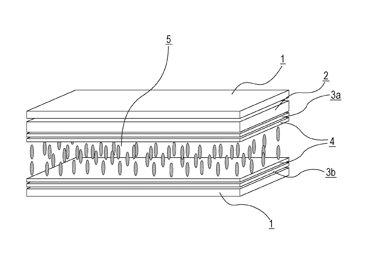
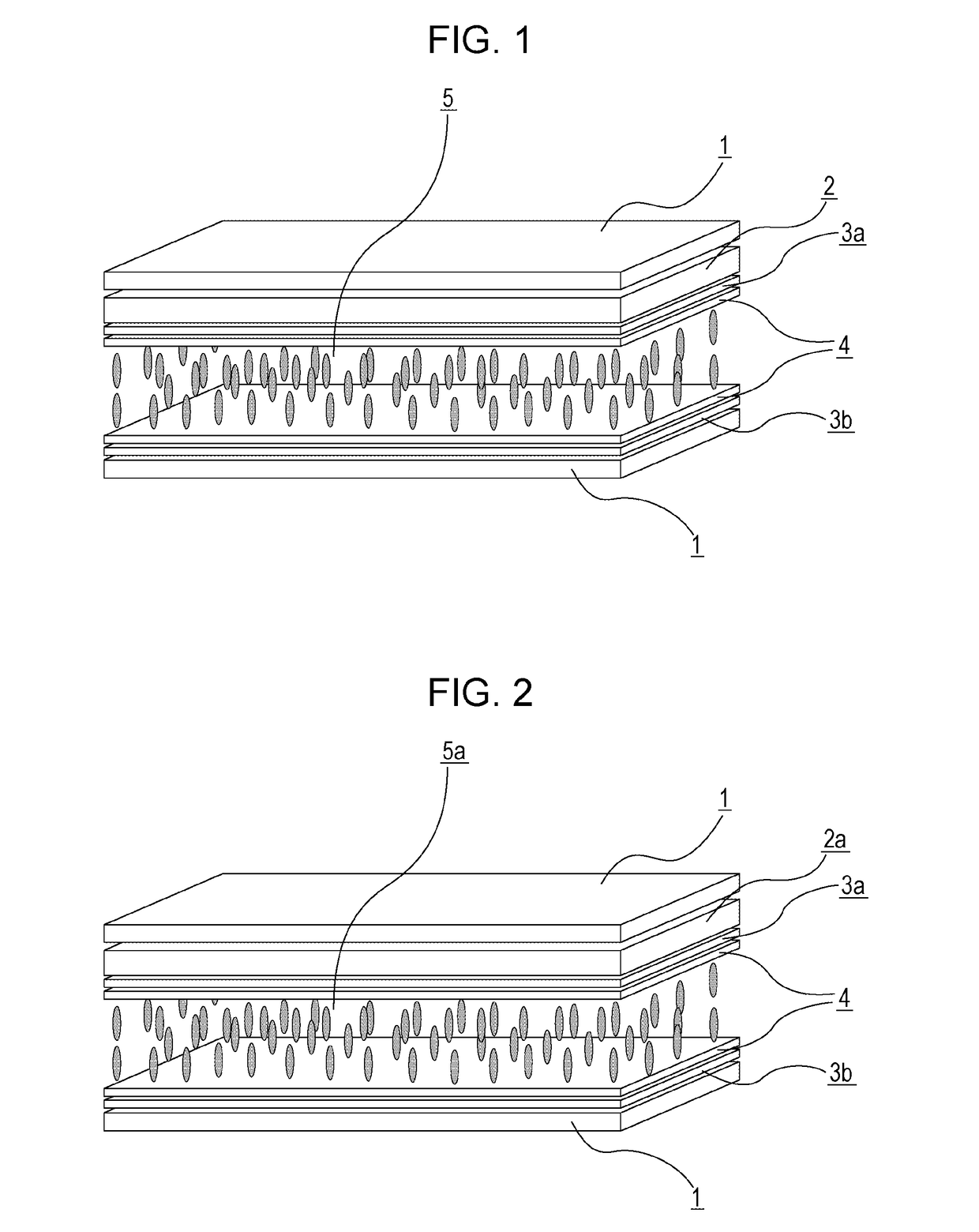
Liquid Crystal Display Device
a liquid crystal display and display device technology, applied in the direction of liquid crystal compositions, instruments, chemistry apparatus and processes, etc., can solve the problems of reducing defective display including voids, and techniques that are not substantially different from merely reducing the impurity content, so as to prevent the decrease of the voltage holding ratio of the liquid crystal layer, the effect of eliminating defective displays
- Summary
- Abstract
- Description
- Claims
- Application Information
AI Technical Summary
Benefits of technology
Problems solved by technology
Method used
Image

Examples
examples
[0203]Although some preferred embodiments of the present invention will now be described in detail with reference to Examples, the present invention is not limited to Examples. In compositions which will be described in Examples and Comparative Examples, the term “%” refers to “mass %”.
[0204]In Examples, the following properties were measured.
[0205]Tni: Nematic phase-isotropic liquid phase transition temperature (° C.)
[0206]Δn: Refractive index anisotropy at 25° C.
[0207]Δ∈: Dielectric anisotropy at 25° C.
[0208]η: Viscosity at 20° C. (mPa·s)
[0209]γ1: Rotational viscosity at 25° C. (mPa·s)
[0210]dgap: Gap between first and second substrates in cell (μm)
[0211]VHR: Voltage holding ratio (%) at 70° C.
[0212](ratio, represented by %, of a measured voltage to the initially applied voltage, which was obtained as follows: a liquid crystal composition was put into a cell having a thickness of 3.5 μm, and the measurement was carried out under the conditions of an applied voltage of 5 V, a frame ...
examples 1 to 7
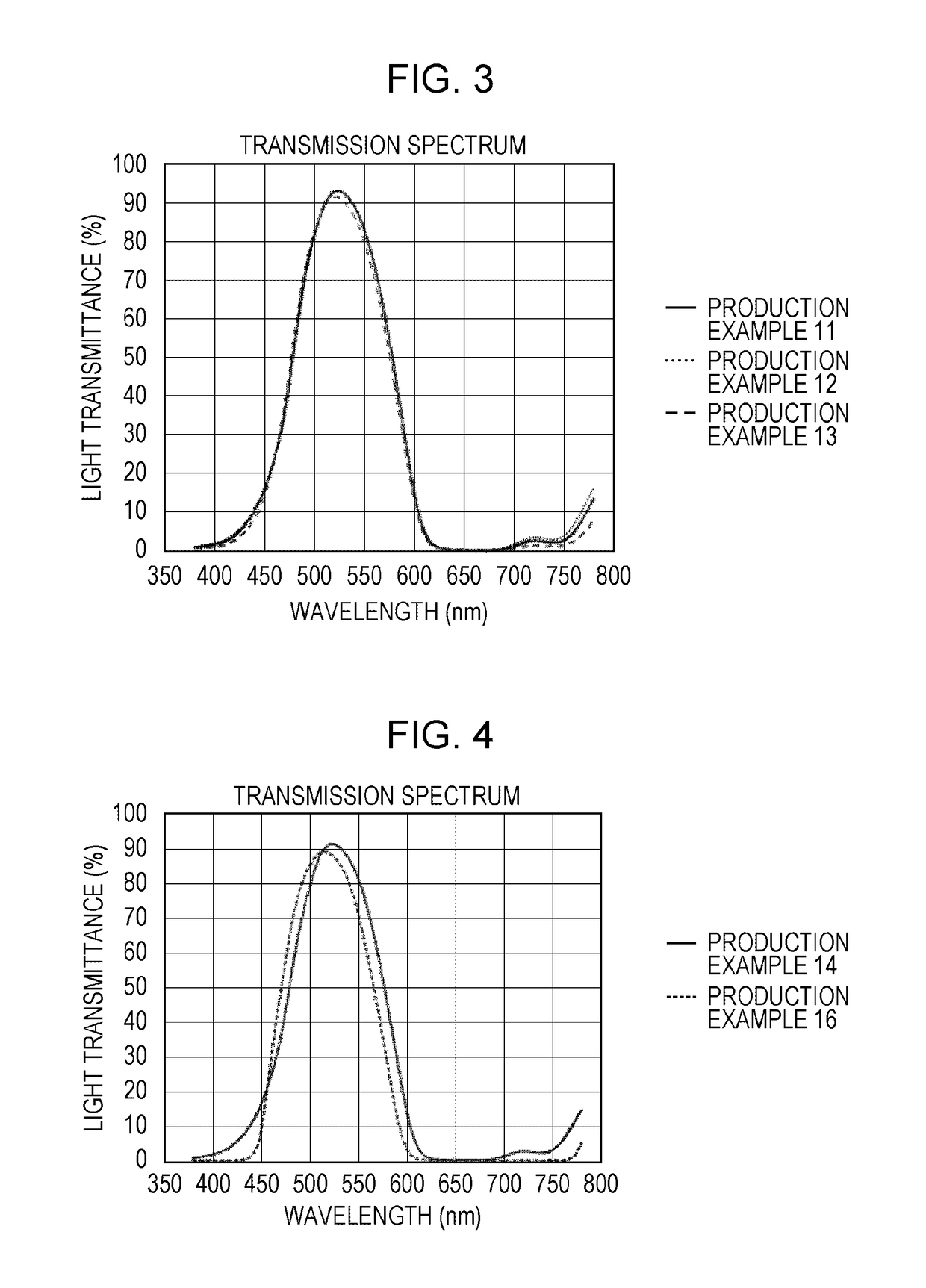
[0267]Electrodes corresponding to first and second substrates were formed, vertical alignment films were formed on the facing surfaces thereof, the alignment films were slightly rubbed to form a VA cell, and then a liquid crystal composition 1 shown in Table 2 was placed between the first and second substrates. Then, the color filters 1 to 5, 7, and 9 shown in Table 1 were used to produce liquid crystal display devices of Examples 1 to 7 (dgap=3.5 μm and alignment film SE-5300). The VHRs and ID of the produced liquid crystal display devices were measured. The liquid crystal display devices were subjected to the evaluation of screen burn-in. Table 3 shows results of the measurement and evaluation.
[0268]
TABLE 2Liquid crystal composition 1TN| / ° C.81.0Δn0.103Δε−2.9η / mPa · s20.3γ1 / mPa · s112γ1 / Δn2 × 10−21053-Cy-Cy-224%3-Cy-Cy-410%3-Cy-Cy-5 5%3-Cy-Ph-O1 2%3-Cy-Ph5-O213%2-Cy-Ph-Ph5-O2 9%3-Cy-Ph-Ph5-O2 9%3-Cy-Cy-Ph5-O3 5%4-Cy-Cy-Ph5-O2 6%5-Cy-Cy-Ph5-O2 5%3-Ph-Ph5-Ph-2 6%4-Ph-Ph5-Ph-2 6%
[026...
examples 8 to 21
[0272]As in Example 1, liquid crystal compositions shown in Table 4 were individually placed between the substrates, the color filters 1 to 5, 7, and 9 shown in Table 1 were used to produce liquid crystal display devices of Examples 8 to 21; and the VHRs and ID thereof were measured. The liquid crystal display devices were subjected to the evaluation of screen burn-in. Tables 5 and 6 show results of the measurement and evaluation.
[0273]
TABLE 4Liquid crystal composition 2Liquid crystal composition 3TN| / ° C.76.0TN| / ° C.84.8Δn0.103Δn0.103Δε−2.9Δε−2.9η / mPa · s19.8η / mPa · s21.4γ1 / mPa · s110γ1 / mPa · s119γ1 / Δn2 × 10−2103γ1 / Δn2 × 10−21123-Cy-Cy-224%3-Cy-Cy-224%3-Cy-Cy-410%3-Cy-Cy-411%3-Cy-Ph-O1 7%3-Cy-Ph5-O212%3-Cy-Ph5-O214%2-Cy-Ph-Ph5-O2 5%2-Cy-Ph-Ph5-O2 7%3-Cy-Ph-Ph5-O2 6%3-Cy-Ph-Ph5-O2 9%3-Cy-Cy-Ph5-O3 8%3-Cy-Cy-Ph5-O3 5%4-Cy-Cy-Ph5-O2 8%4-Cy-Cy-Ph5-O2 7%5-Cy-Cy-Ph5-O2 8%5-Cy-Cy-Ph5-O2 5%3-Ph-Ph5-Ph-2 6%3-Ph-Ph5-Ph-2 6%4-Ph-Ph5-Ph-2 6%4-Ph-Ph5-Ph-2 6%5-Ph-Ph-1 3%3-Cy-Cy-Ph-1 3%
[0274]
TABL...
PUM
| Property | Measurement | Unit |
|---|---|---|
| volume fraction | aaaaa | aaaaa |
| particle size | aaaaa | aaaaa |
| temperature | aaaaa | aaaaa |
Abstract
Description
Claims
Application Information