Selective and conformal passivation layer for 3D high-mobility channel devices

a passivation layer and high-mobility channel technology, applied in semiconductor devices, semiconductor/solid-state device details, electrical apparatus, etc., can solve the problem of process reaction-limited instead of diffusion-limited, and achieve the effect of reducing the deposit rate and increasing the deposition ra

Inactive Publication Date: 2018-05-29
IBM CORP +1
View PDF10 Cites 6 Cited by
  • Summary
  • Abstract
  • Description
  • Claims
  • Application Information

AI Technical Summary

Benefits of technology

[0007]Next a SixH(2x+2) based deposition process up to a temperature of 400 degrees Celsius is applied on the first layer, and the second layer thereby f

Problems solved by technology

This makes the process reaction-limited instead of dif

Method used


Image

  • Selective and conformal passivation layer for 3D high-mobility channel devices
  • Selective and conformal passivation layer for 3D high-mobility channel devices
  • Selective and conformal passivation layer for 3D high-mobility channel devices

Examples


Embodiment Construction

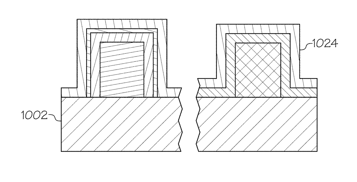
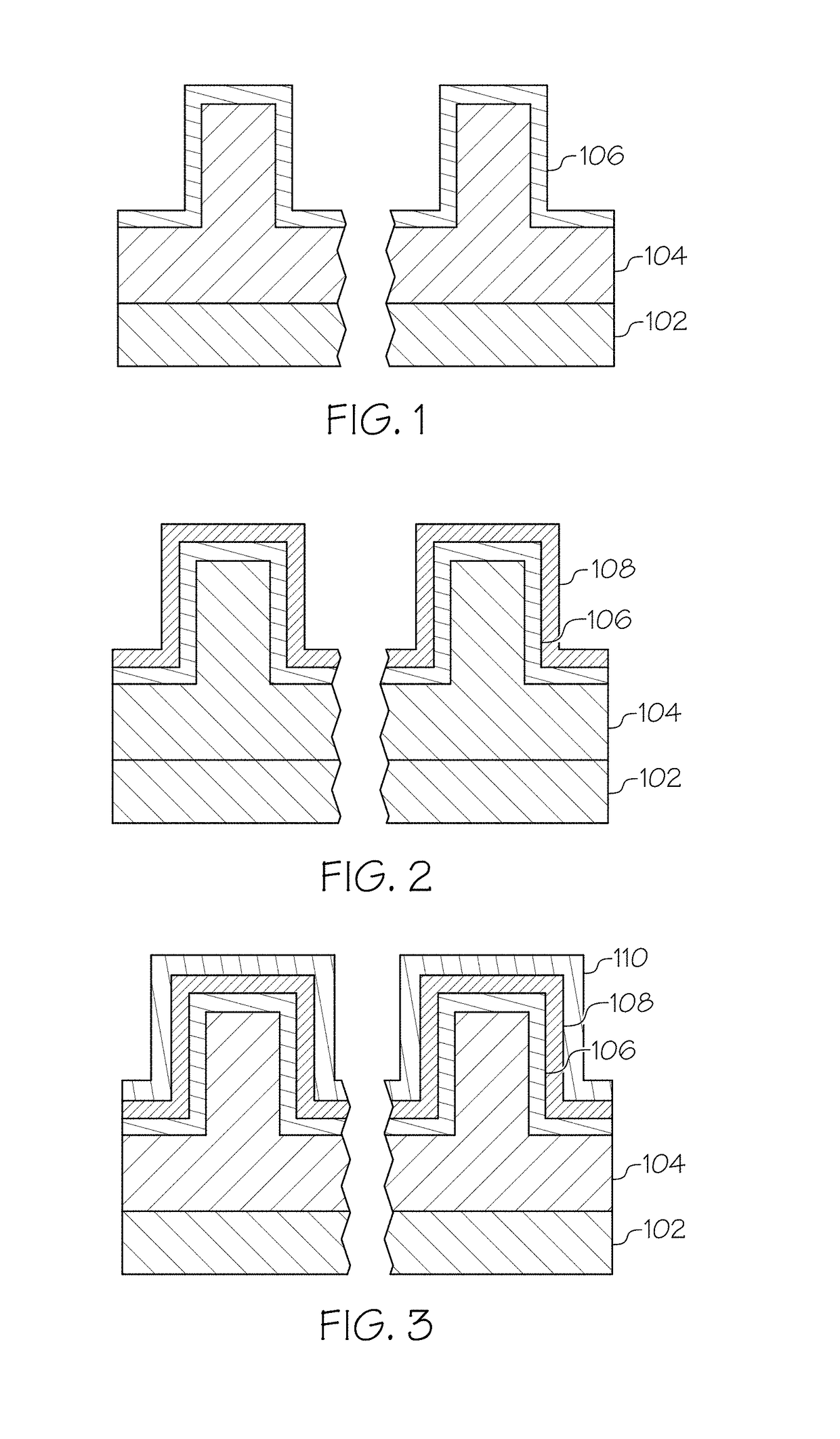
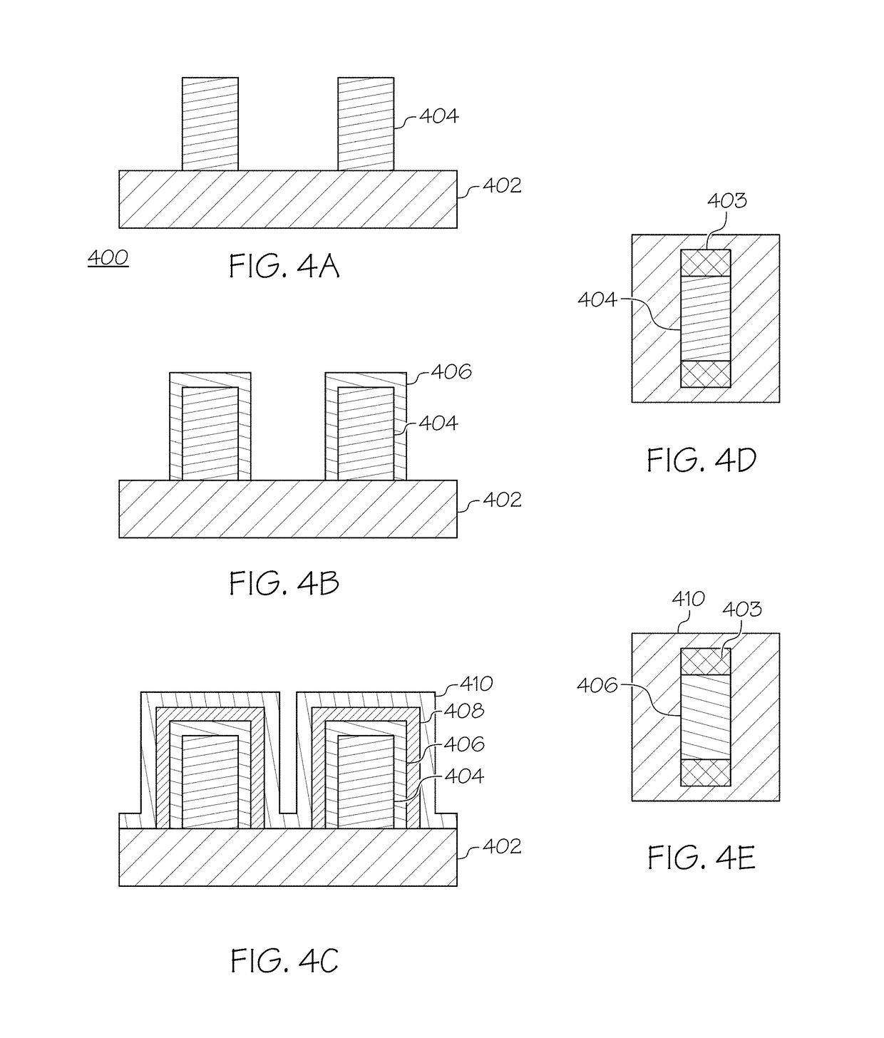
[0022]It is to be understood that the present invention will be described in terms of a given illustrative example process for surface conditioning of semiconductor interfaces, junctions, and contacts. However, other semiconductor architectures, structures, substrate materials, and process features and steps can be varied within the scope of the present invention.

[0023]The present invention provides a scaled dielectric stack interlayer, compatible with subsequent high temperature processing with good electrical transport & reliability properties.

Non-Limiting Definitions

[0024]The terms “a”, “an” and “the” preceding an element or component are intended to include the plural forms as well, unless the context clearly indicates otherwise.

[0025]The terms “comprises”, “comprising”, “includes”, “including”, “has”, “having”“contains” or “containing” or any other variation thereof, are intended to cover a non-exclusive inclusion. For example, a composition, a mixture, process, method, article...


PUM


Abstract

A scaled dielectric stack interlayer, compatible with subsequent high temperature processing with good electrical transport & reliability properties is provided. A method for forming a conformal aSi:H passivation layer on a semiconductor device is described. A patterned semiconductor wafer is placed in in a process chamber with a first layer formed thereon and a second layer formed thereon, the first layer and the second layer being two different materials Next, a SixH(2x+2) based deposition up to a temperature of 400 degrees Celsius is used on the first layer and the second layer thereby forming a conformal aSi:H passivating layer is formed at a higher rate of deposition on the first layer selectively and a lower rate of deposit on the second layer.

Description

BACKGROUND OF THE INVENTION[0001]The present invention relates to semiconductor devices, and more specifically, to the deposition of materials on high-mobility semiconductor layers.[0002]Highly scaled device architecture such as FinFETs and Nanowires require a conformal high-quality gate stack to enable uniform electrostatic control. This is particularly challenging for the key interface layer of high mobility semiconductors such as InGaAs or (Si)Ge which possess low quality native oxides and have limited temperature process windows of up to 400 and 800 degrees Celsius, respectively, when their surfaces is exposed. In addition, monolithic CMOS integration with dual channels, e.g. InGaAs nFET & (Si)Ge pFET, generate complexity and limiting the number of process steps including lithography, masking, and etching by using deposition selectivity will reduce cost and increase yield.SUMMARY OF THE INVENTION[0003]In one embodiment, a process for forming a passivating conformal aSi:H interla...

Claims


Application Information

Patent Timeline
IPC IPC(8): H01L21/02H01L23/29H01L27/12H01L23/31H01L29/78H01L21/84H01L21/28
CPCH01L21/845H01L23/3171H01L23/298H01L21/02123H01L23/3192H01L21/0206H01L21/02323H01L21/02359H01L21/28008H01L29/785H01L27/1211H01L21/02164H01L21/0214H01L21/02181H01L21/02178H01L21/02192H01L21/28158H01L21/28255H01L21/28264H01L21/0228H01L21/02304H01L21/823821H01L29/66795H01L27/0924H01L29/1054
Inventor CHU, JACK O.GATES, STEPHEN M.HATANAKA, MASANOBUNARAYANAN, VIJAYNEUMAYER, DEBORAH A.OGAWA, YOHEIROZEN, JOHN
Owner IBM CORP
Why Eureka
Try Eureka