Field emission cathode having an electrically conducting material shaped of a narrow rod or knife edge

a field emission cathode and narrow rod technology, applied in the direction of cold cathodes, liquid electrodes of discharge tubes, electrolyte emitting electrodes/cathodes, etc., can solve the problem that the field emission cathodes of vacuum microelectronics cannot be produced in their optimal geometry, the electric stream declines with the operating time, and the method is impractical, so as to achieve high emission quality and long life

Inactive Publication Date: 2003-08-19
KEESMANN TILL
View PDF4 Cites 49 Cited by
  • Summary
  • Abstract
  • Description
  • Claims
  • Application Information

AI Technical Summary

Benefits of technology

The present invention is based on the object or on the technical problem of specifying a field emission cathode which avoids the disadvantages of the prior art, assures high emission quality, makes possible a longer lifetime, and in particular resists bombardment with residual gas ions. Furthermore, the present invention is based on the object or on the technical problem of specifying a method for producing a field emission cathode of the type mentioned in the introduction, so as to assure technically optimal manufacture together with economy.
Using well-known carbon nano-cylinders as a field emission cathode thus combines the advantage of optimal geometry with high strength, thus assuring that the emission properties of such field emission cathodes will not change during their operation, in contrast to previously used cathode tips.

Problems solved by technology

A disadvantage in the use of tips and edges, which have been produced by the known methods, is that the electron stream declines with operating time, since the tips or edges are destroyed by the positive ions of the unavoidable residual gas in the system.
Furthermore, field emission cathodes for vacuum microelectronics cannot be produced in their optimal geometry by the prior art.
However, this method is impractical, and in particular is not suited for field electron arrays with many cathode tips, as is desired in vacuum microelectronics.

Method used


Image

  • Field emission cathode having an electrically conducting material shaped of a narrow rod or knife edge
  • Field emission cathode having an electrically conducting material shaped of a narrow rod or knife edge
  • Field emission cathode having an electrically conducting material shaped of a narrow rod or knife edge

Examples


Embodiment Construction

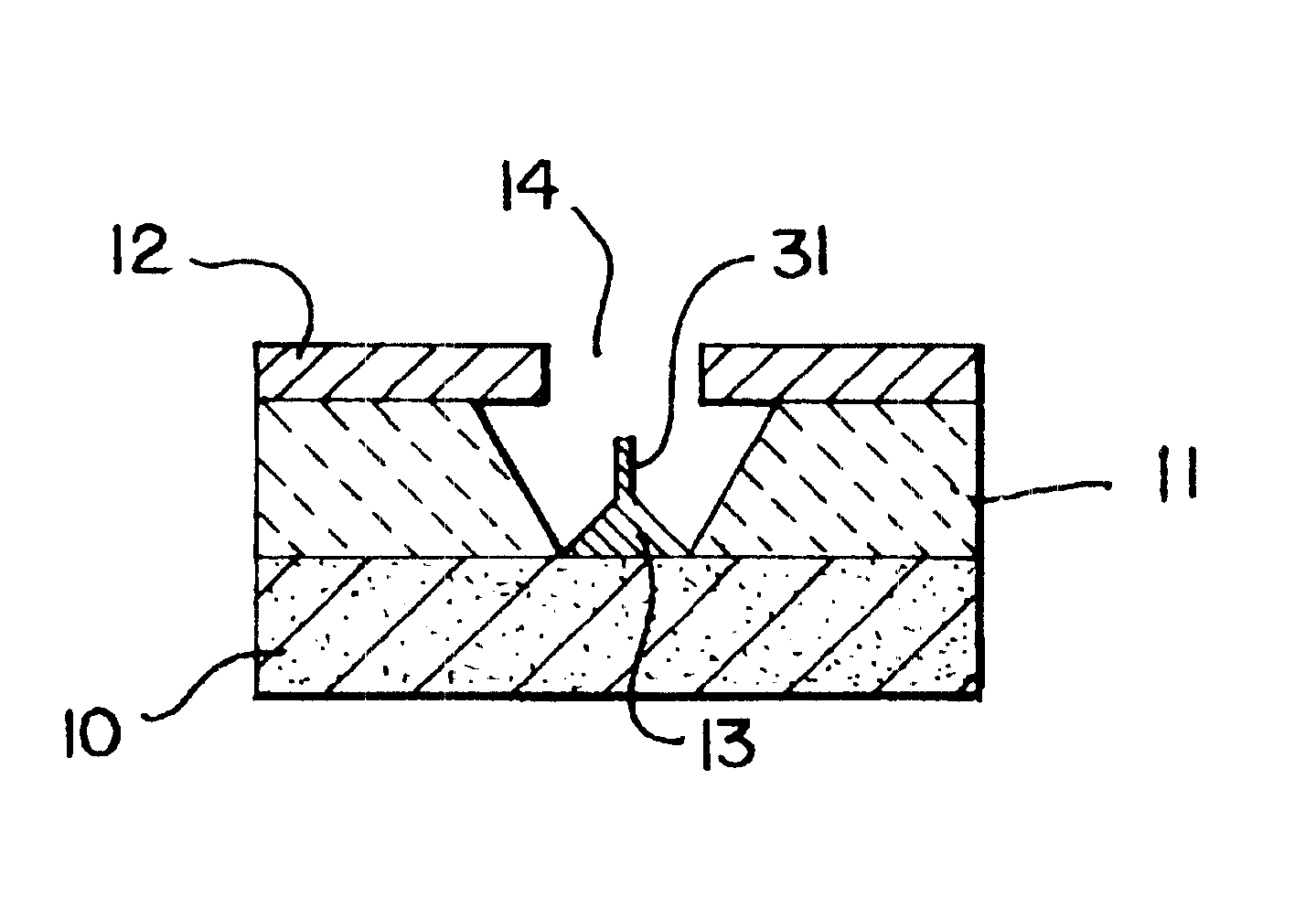
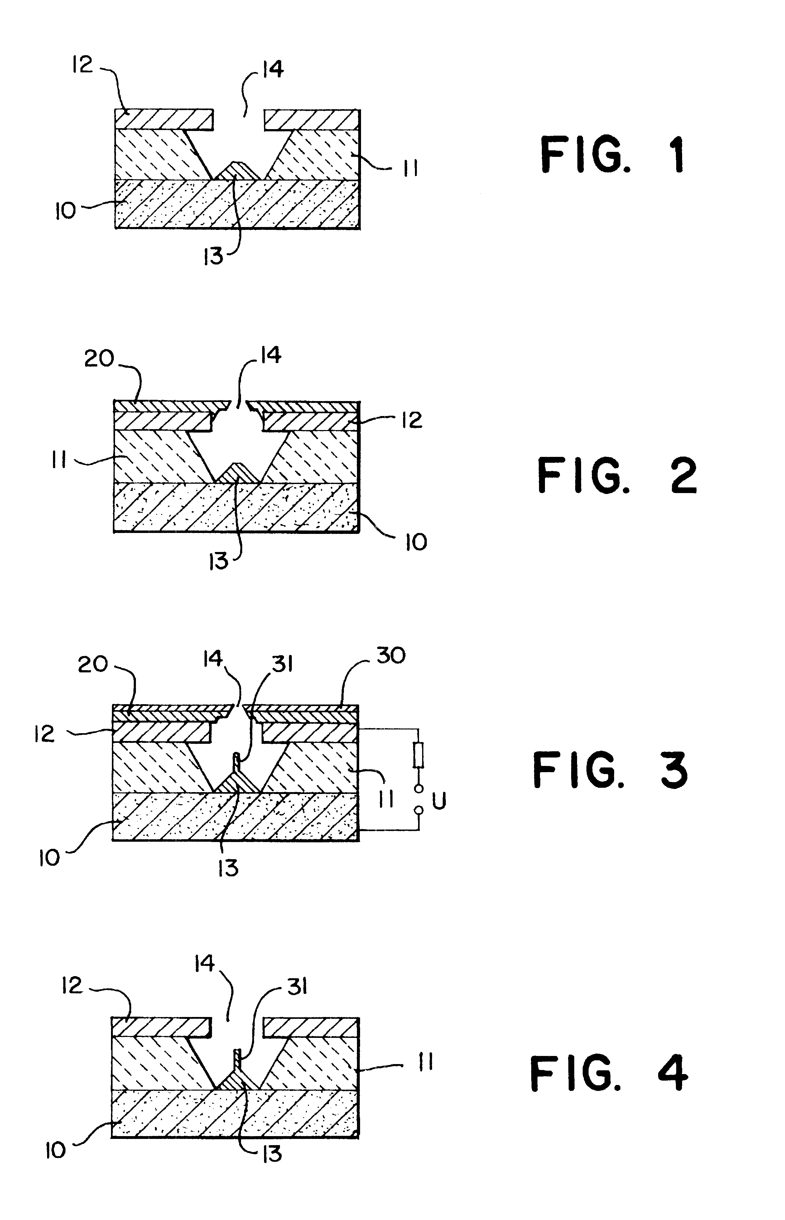
Below it will be explained, by way of an example, how field emission cathodes of carbon nano-cylinders can be produced, such as can be used, for example, as cathodes for diodes or switches. By way of a second example, it will be explained how field emission cathodes for a field emitter array can be produced by the methods of microstructure technology.

Example: Production of individual cathodes on a knife edge

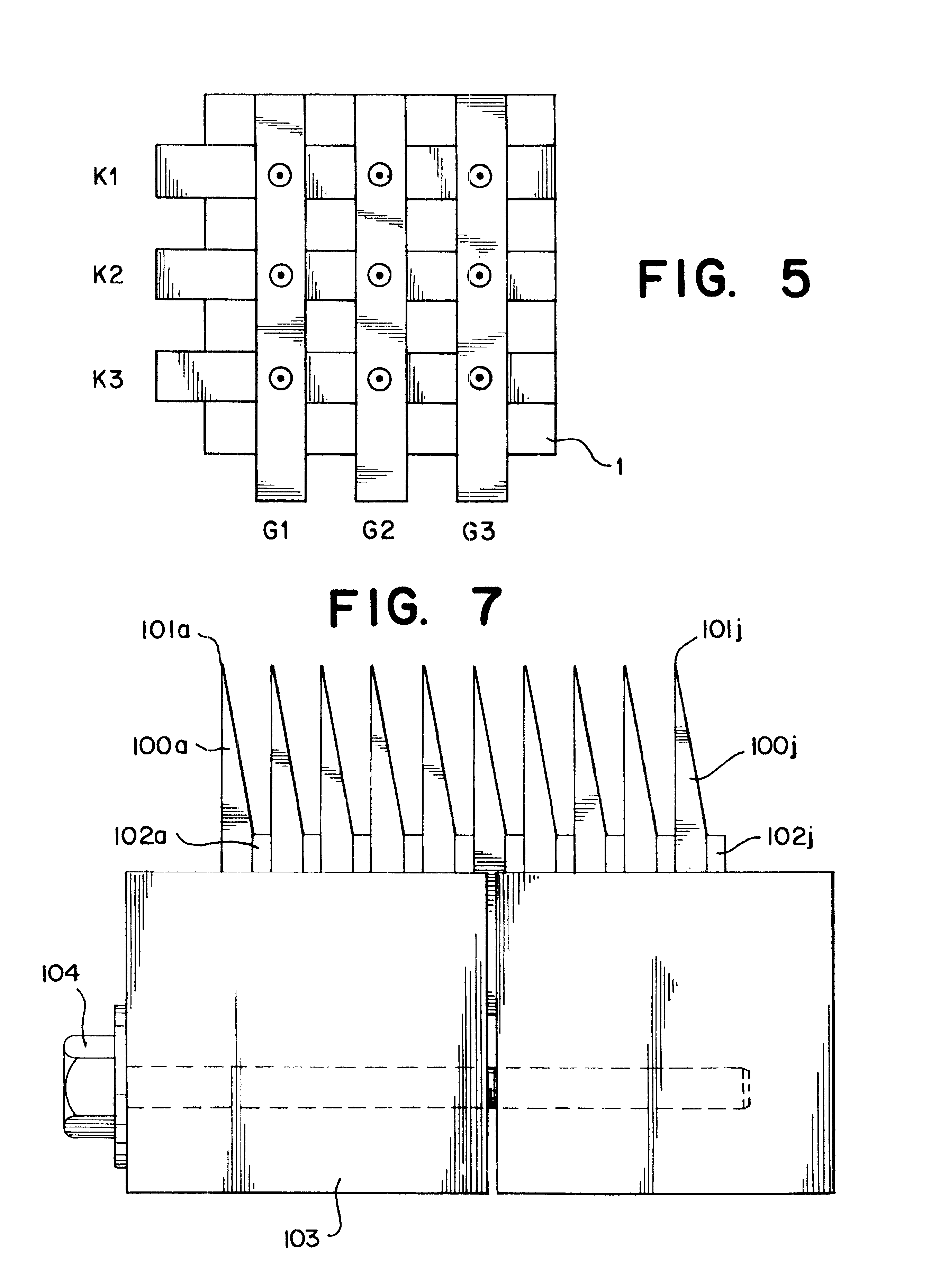
Square graphite wafers about 1 cm (centimeter) on a side, and 1 mm (millimeter) thick are ground or etched to a knife edge on one side. FIG. 6 shows such a graphite wafer 100 with a knife edge 101, beveled on one side. FIG. 7 shows how ten of these graphite wafers 100a to 100j are collected together into a block in a clamping fixture 103, in such a way that the knife edges 101a to 101j on one side of the block lie in one plane and an aluminum foil or Teflon foil is situated between each of the graphite wafers as a spacer 102a to 102j. The clamping fixture consists of two brass bl...


PUM


Abstract

A field emission cathode device consisting of an electrically conducting material and with a narrow, rod-shaped geometry or a knife edge, to achieve a high amplification of the electric field strength is characterized in that the electron-emitting part of the field emission cathode at least partly has preferred cylindrical host molecules and / or compounds with host compounds and / or cylindrical atomic networks, possibly with end caps with diameters measuring in the nanometer range.

Description

The invention relates to a field emission cathode device of an electrically conducting material and with a narrow, rod-shaped geometry or a knife edge to achieve high amplification of the electric field strength, such that the electron-emitting part of the field emission cathode has cylindrical molecules. The invention also relates to a method for producing such a field emission cathode device.Field emission means the emission of electrons from the surface of an electric conductor under the action of an electric field exceeding 10.sub.9 V / m. In practice, such field strengths are realized at sharp edges or tips, where the field strength is amplified. High vacuum is necessary to avoid gas discharges.DESCRIPTION OF THE PRIOR ARTField emission cathodes are used, for example, in field electron microscopes, in electron accelerators, in high-power switches (OS DE 39 24 745 A1) and in field emission diodes and field emitter arrays for vacuum microelectronics (thus for example Busta, Vacuum ...

Claims


Application Information

Patent Timeline
Patent Type & Authority Patents(United States)
IPC IPC(8): H01J1/304H01J1/30H01J9/02
CPCB82Y10/00H01J1/3042H01J2201/30423H01J2201/30469Y10S977/939Y10S977/876
Inventor KEESMANN, TILLGROSSE-WILDE, HUBERT
Owner KEESMANN TILL
Why Eureka
Try Eureka