Dual-node capacitor coupled MOSFET for improving ESD performance

a mosfet transistor and dual-node technology, applied in the direction of pulse automatic control, pulse technique, semiconductor devices, etc., can solve the problems of gate electrode damage, ic chip damage, oxide layer, etc., and achieve the effect of improving the uniform turn-on of a multi-finger mosfet transistor and lowering the trigger voltag

Inactive Publication Date: 2003-11-18
WINBOND ELECTRONICS CORP
View PDF8 Cites 15 Cited by
  • Summary
  • Abstract
  • Description
  • Claims
  • Application Information

AI Technical Summary

Benefits of technology

The present invention overcomes the deficiencies of the prior art. Specifically, a dual-node capacitor coupling technique is used to lower the trigger voltage and to improve the uniform turn-on of a multi-finger MOSFET transistor.

Problems solved by technology

Electrostatic discharges (ESDs) from human handling of a metal-oxide semiconductor (MOS) IC chip, or from other causes, permanently damage the IC chip.
Often the thin-oxide layer that isolates the gate electrode from the substrate of a MOS field effect transistor is irreparably ruptured by a voltage spike applied across it.
Submicron CMOS devices, such as short channel thin-oxide MOS devices, are extremely susceptible to ESD damage.
This occurs when a strong electric field across the depletion region in the drain substrate junction becomes high enough to begin avalanche breakdown, which in turn causes impact ionization, resulting in the generation of both minority and majority carriers.
For manufacturing purposes, however, layout area is typically at a premium, and a conventional long-finger structure may not fit in the designated layout area.

Method used


Image

  • Dual-node capacitor coupled MOSFET for improving ESD performance
  • Dual-node capacitor coupled MOSFET for improving ESD performance
  • Dual-node capacitor coupled MOSFET for improving ESD performance

Examples


Embodiment Construction

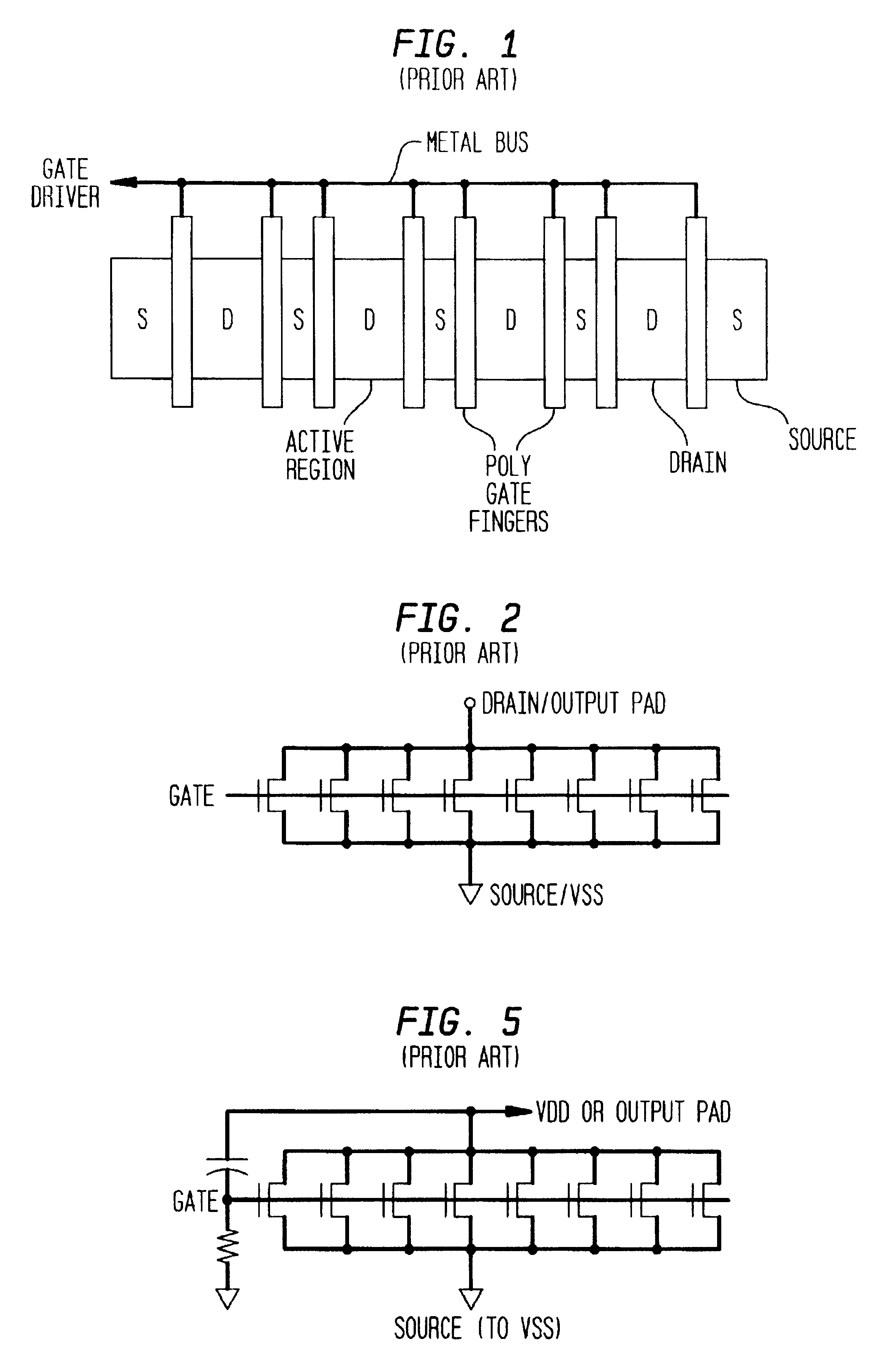
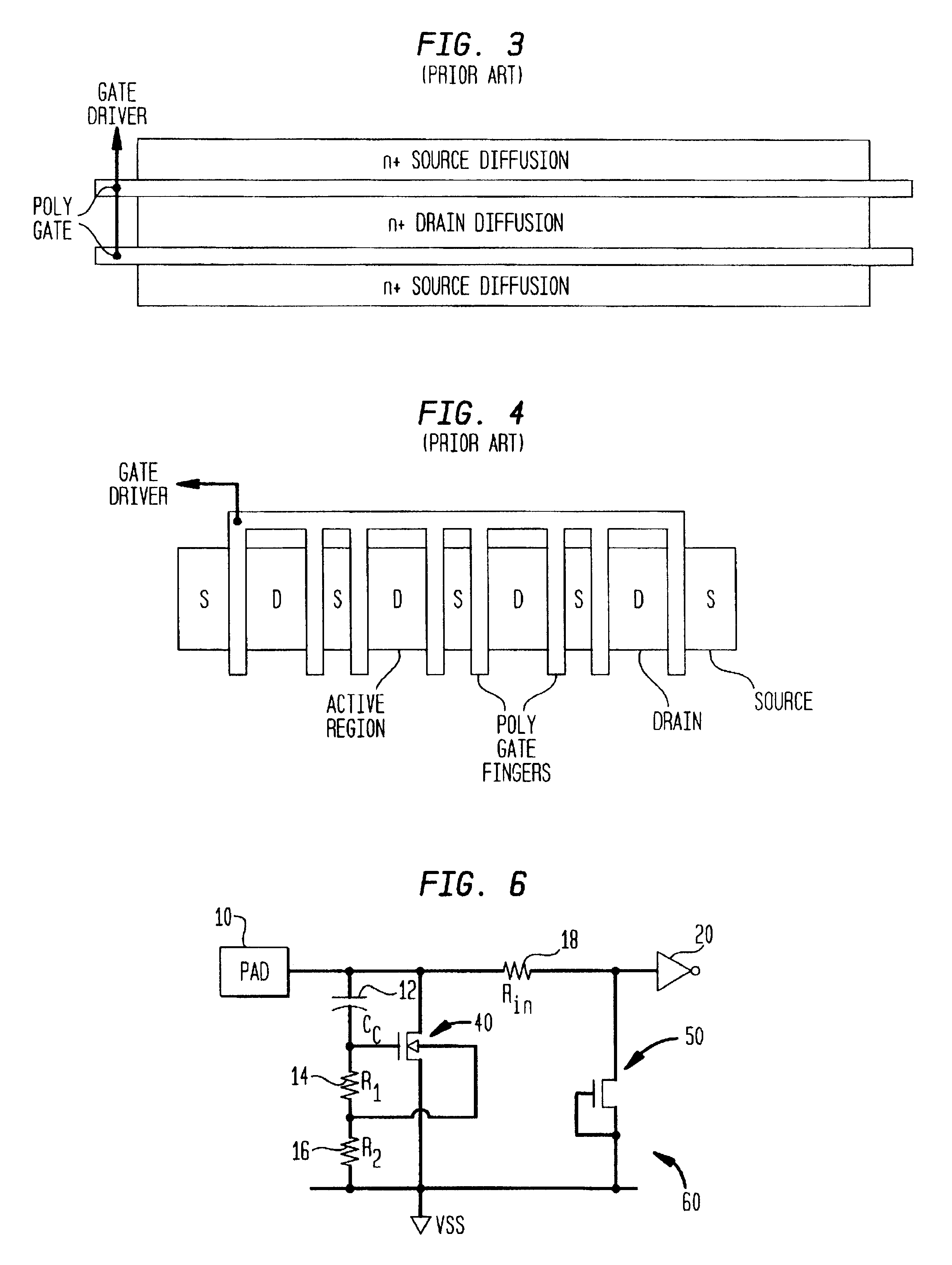
The present invention improves over conventional gate-coupling and well-coupling techniques in that the embodiments provide a lower trigger voltage for each MOSFET in the multi-finger MOSFET device, while improving the turn-on consistency for each MOSFET. Note that, although the present invention is particularly well suited to a multi-finger MOSFET ESD protection device, the present invention may also be employed in a single MOSFET device while providing stellar results.

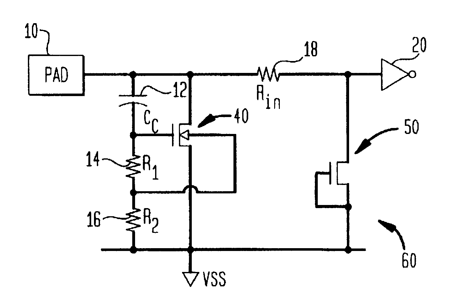
FIG. 6 shows an ESD protection device 60 having a dual-node capacitor in accordance with a first embodiment of the present invention. Protection device 60 is positioned between an IC pad terminal 10 and a buffer 20 that connects to an internal circuit (not shown) to be protected from an ESD event.

Device 60 includes a primary protection circuit that includes MOSFET 40, capacitor 12, and first and second resistors 14, 16, respectively. Illustratively, MOSFET 40 is an NMOS transistor but as previously discussed, may be ...


PUM


Abstract

A dual-node capacitor coupling technique is used to lower the trigger voltage and to improve the uniform turn-on of a multi-finger MOSFET transistor. Preferably, each MOSFET is an NMOS device. Specifically, each NMOS device includes a capacitor that is connected between the gate of the NMOS device and the pad terminal. A first resistor is connected between the gate and the p-well, while a second resistor is connected between the p-well and the grounded source. For a positive ESD pulse to VSS, the p-well is pulled up to approximately 0.7 V during the initial ESD event, such that the source junction is forward biased and that the trigger voltage of the NMOS device is lowered. At the same time the gate voltage is coupled within the range of approximately 1 to 2 V to promote the uniform turn on of the gate fingers of the NMOS devices during the initial ESD event.

Description

FIELD OF THE INVENTIONThe present invention relates to a primary ESD protection circuit, and more particularly, the present invention relates to a primary ESD protection circuit having a dual-node capacitor coupled multi-finger NMOSFET structure.BACKGROUND OF THE INVENTIONElectrostatic discharges (ESDs) from human handling of a metal-oxide semiconductor (MOS) IC chip, or from other causes, permanently damage the IC chip. Often the thin-oxide layer that isolates the gate electrode from the substrate of a MOS field effect transistor is irreparably ruptured by a voltage spike applied across it. A voltage spike or ESD is often applied to the gate, because the gate electrode is connected to an external terminal or pin of the IC chip. The external terminals are formed on an input or output pad. To prevent such damage from excessive electrostatic discharges, a protective device is often connected between the pad and the internal circuits.As CMOS technology is scaled down into submicron reg...

Claims


Application Information

Patent Timeline
Patent Type & Authority Patents(United States)
IPC IPC(8): H01L27/02
CPCH01L27/0251H01L2924/0002H01L2924/00
Inventor LIN, SHIN-TRONWONG, SHYH-CHYI
Owner WINBOND ELECTRONICS CORP
Why Eureka
Try Eureka