Semiconductor switching apparatus and method of controlling a semiconductor switching element

Inactive Publication Date: 2005-05-17
MITSUBISHI ELECTRIC CORP
View PDF2 Cites 0 Cited by
  • Summary
  • Abstract
  • Description
  • Claims
  • Application Information

AI Technical Summary

Benefits of technology

[0027]The first object of the present invention is to prevent the dissipation from locally concentrating on part of semiconductor switching elements within the semiconductor wafer. That avoids the failure of the device, to thereby enhance the reliability of the apparatus.
[0028]The second object of the present invention is to prevent or markedly suppress the dissipation caused by the snubber circuit in the background art. That ensures size-reduction, simplification, cost-reduction and high efficiency of the apparatus.
[0029]The third object of the present invention is to eliminate the necessity for a circuit to suppress a rise in the voltage between the first and second electrodes, such as a snubber circuit. That ensures size-reduction of the apparatus and high efficiency.

Problems solved by technology

The spike voltage VDSP is likely to cause a dissipation.
(1) As shown in FIG. 19, the external gate lead 21P which draws the gate reverse current is taken out from a localized portion inside the ring-shaped gate electrode 34P. Accordingly, only one-way drawing of the gate reverse current is made. As a result, when the GTO is turned off, with nonuniform cathode current, the loss produced by the spike voltage and the tail current, i.e., dissipation, is locally concentrated on the cathode side surface inside the GTO, the GTO device is failed by a local rise of temperature, to fall into a conductive state. Thus, there arises a problem that failure of the turn-off occurs with high probability.
(2) The second problem is caused by the snubber circuit, in particular, the snubber capacitor.
Thus, when the GTO 3P is connected to the snubber resistor which has the above capacitance of power consumption, the power generated by the snubber resistor is out of the power to be transmitted as a loss to degrade the efficiency, and further the necessity for the cooling device arises.
That is a hindrance to simplification and size-reduction of the whole apparatus.

Method used


Image

  • Semiconductor switching apparatus and method of controlling a semiconductor switching element
  • Semiconductor switching apparatus and method of controlling a semiconductor switching element
  • Semiconductor switching apparatus and method of controlling a semiconductor switching element

Examples


Embodiment Construction

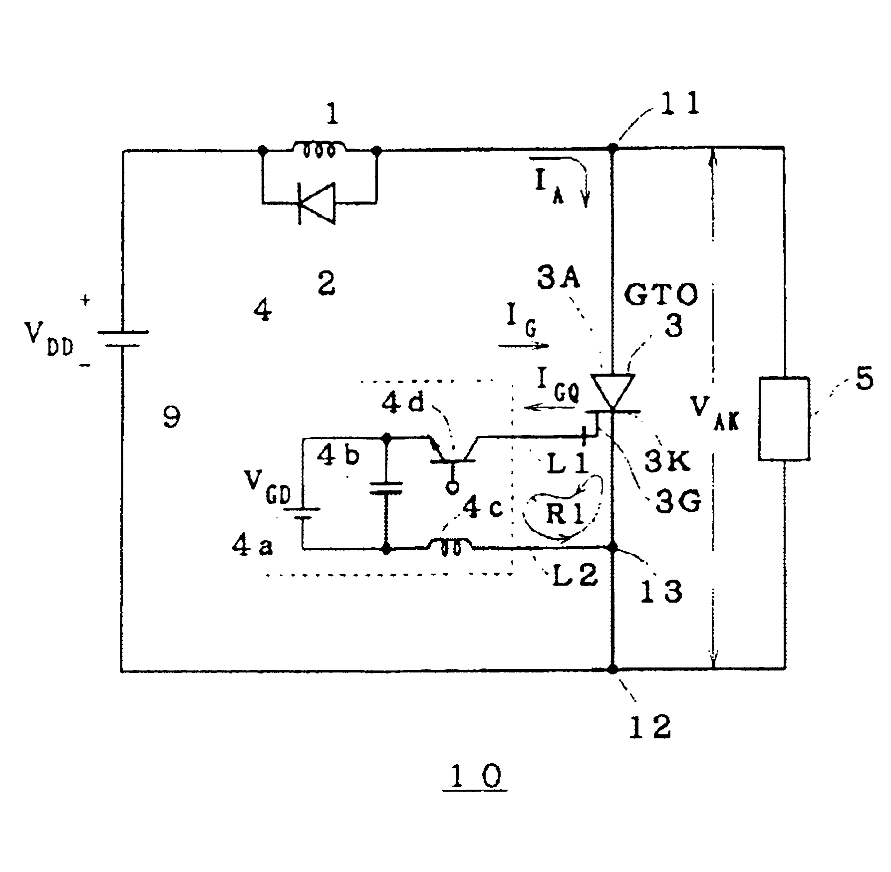
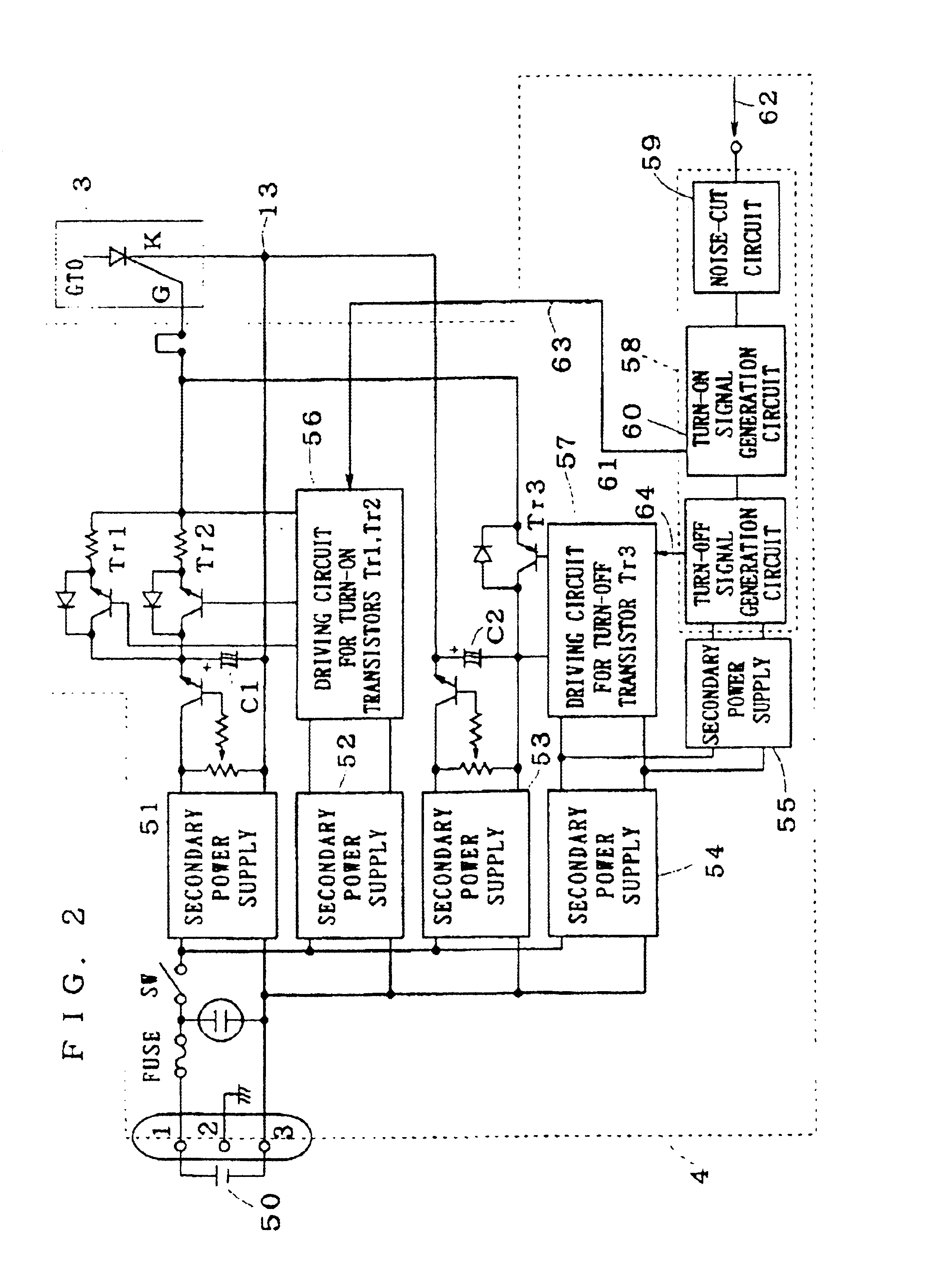
[0049]A semiconductor switching apparatus or a semiconductor switching element is applied for various types of power converters, such as a power converter on traction, an SVG (Static Var Generator) and an industrial power converter.

[0050]The point of the proposed new method of controlling the semiconductor switching element (or switching device) lies in that a main current flowing in the semiconductor switching element in an on-state is entirely commutated to a driving circuit, to thereby bring the semiconductor switching element into a turn-off state.

[0051]A gate turn-off thyristor (hereinafter referred to as “GTO”) will be discussed as an example of the semiconductor switching element. In this case, the first, second and third electrodes of the GTO correspond to an anode electrode, a cathode electrode and a gate electrode, respectively. The semiconductor switching element is not limited to the GTO of a quadruple layered structure, but may be a transistor of a triple layered struct...


PUM


Abstract

An inductance in a path (R1) from a gate electrode (3G) of a GTO (3) through a gate driver (4) and a node (13) to a cathode electrode (3K) is determined so that a turn-off gain may be not more than 1. At a turn-off, a main current (IA) is entirely commutated from the gate electrode (3G) towards the node (13) through the gate driver (4) in a direction reverse to a turn-off control current (IG) A peak voltage suppressing circuit (5) clamps an anode-cathode voltage (VA-K) which rises on, to a prescribed voltage value for a prescribed time. This prevents losses caused by a snubber circuit. Commutation of a main current to the gate prevents locally concentrating in the cathode side of the semiconductor switching element, to thereby increase the turn off capability of the semiconductor switching element. Further, this prevents or reduces dissipation of large amount produced by a discharge of the electric charges from a snubber capacitor. Thus, reduction in dissipation and in size of the whole apparatus can be achieved.

Description

BACKGROUND OF THE INVENTION[0001]1. Field of the Invention[0002]The present invention relates to a semiconductor switching apparatus used for e.g., a power converter, and to a method of controlling a semiconductor switching element.[0003]2. Description of the Background Art[0004]FIG. 16 is a diagram showing an example of a circuit configuration of a prior-art semiconductor switching apparatus. In FIG. 16, a semiconductor switching apparatus is given reference character 3P, which is herein a GTO (Gate Turn-off Thyristor). A gate driver 4P connected between the gate and cathode of GTO 3P produces a gate turn-on control current IGP and applies the current IGP to the gate of GTO 3P to turn the GTO 3P on. Further, the driver 4P conducts a gate reverse current IGQP whose rate of rise of current (dIDQP / dt) is in a range of 20 to 50 A / μs from the gate to the cathode of GTO 3P. The gate reverse current Igqp is separated from the anode current IAP. At this time, a turn-off gain ranges from 2 ...

Claims


Application Information

Patent Timeline
IPC IPC(8): H03K17/72H01L29/744H01L29/74H02M1/06H03K17/0812H03K17/0814H03K17/16H03K17/732
CPCH03K17/08124H03K17/08144H03K17/16H03K17/732
Inventor KURACHI, KAZUHIROYAMAMOTO, MASANORI
Owner MITSUBISHI ELECTRIC CORP
Why Eureka
Try Eureka