
Calibration of isolated analog-to-digital converters

an analog-to-digital converter and calibration technology, applied in the field of analog-to-digital converter calibration, can solve the problems of difficult calibration of adc, inability to provide each adc with a precise reference, and gain and offset of individual channels, so as to eliminate the effects of drift in the different channels and eliminate the effect of selected gain and offset effects

Inactive Publication Date: 2008-02-26
CIRRUS LOGIC INC
View PDF7 Cites 1 Cited by
  • Summary
  • Abstract
  • Description
  • Claims
  • Application Information

AI Technical Summary

Benefits of technology

[0019]Related measurement data collected by isolated analog-to-digital converters in multiple channels may be transmitted to a microprocessor or programmable logic device for centralized processing, to eliminate selected gain and offset effects common to the different analog-to-digital converters in the different channels, eliminating the consequences of drift in the different channels.
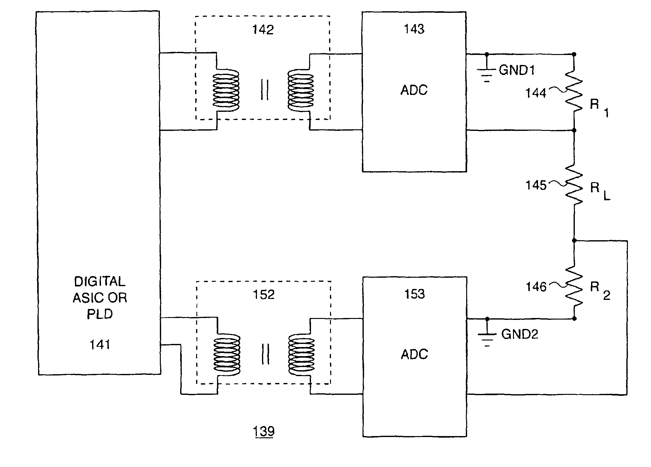
[0020]In particular, a pair of precision resistors is provided to calibrate the different channels. The ADCs may be factory calibrated and the ratio between the two precision resistors stored within the ADCs. The ADCs may later self-calibrate by comparing their relative gains to the stored resistor ratio. Gain of one of the ADCs may be adjusted relative to the other in order to maintain a relative gain calibration. Although absolute gain is not calibrated (as the resisters are isolated) for particular applications, only relative gain between the ADCs is relevant. Thus, the present invention provides a cost-effective and simple solution to relative gain calibration between isolated ADCs.

Problems solved by technology

The gain and offset of individual channels relative to one another is an issue which may require attention.
Such applications are precise, cost-sensitive applications where providing each ADC with a precise reference is not an affordable solution.
However, such isolation barriers may make it difficult to calibrate the ADC since the microcontroller or programmable logic device may have difficulty sending a precise voltage reference signal through the isolation barrier.
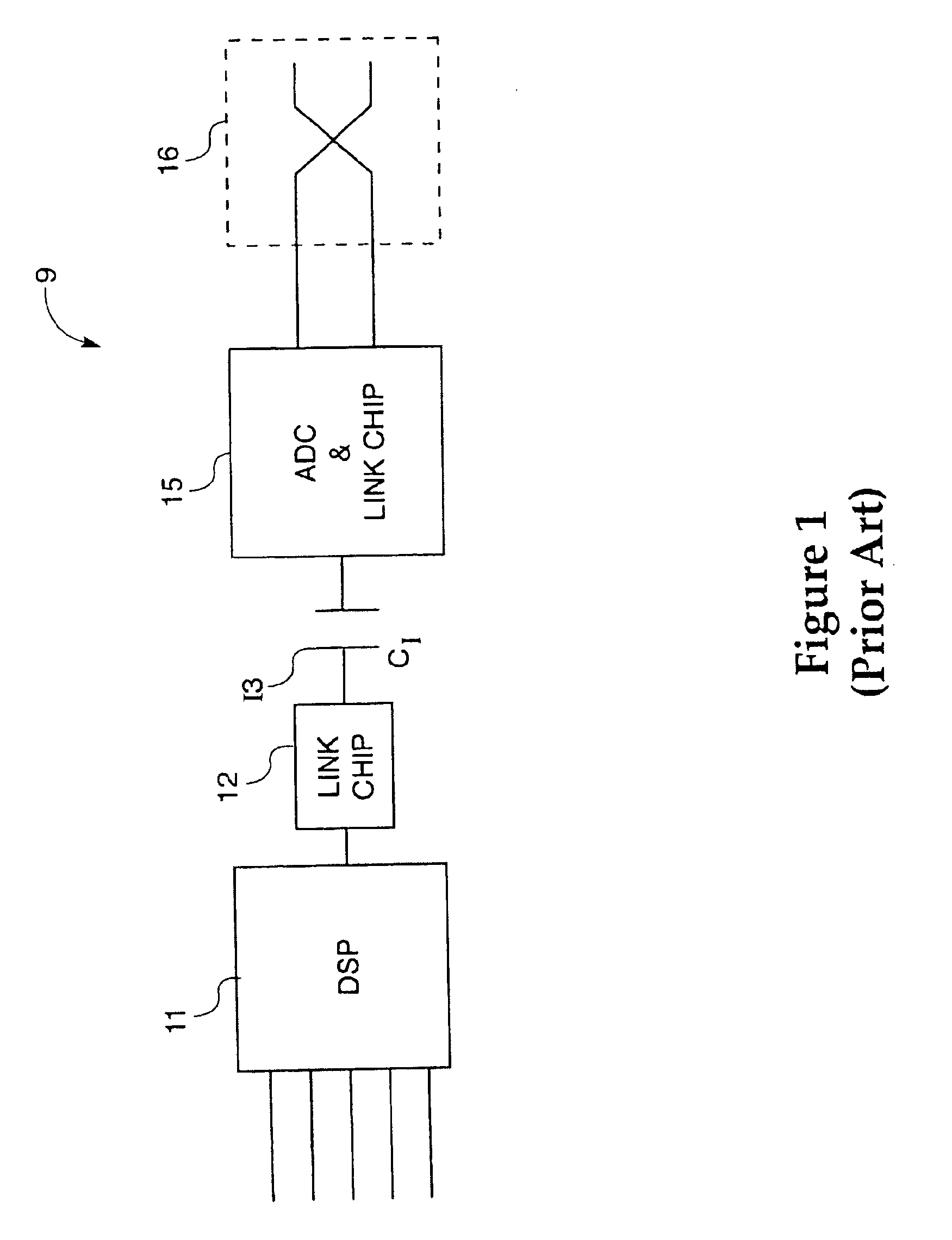
In the prior art, additional signal lines may be required for such additional signals, increasing the complexity and cost of the device.
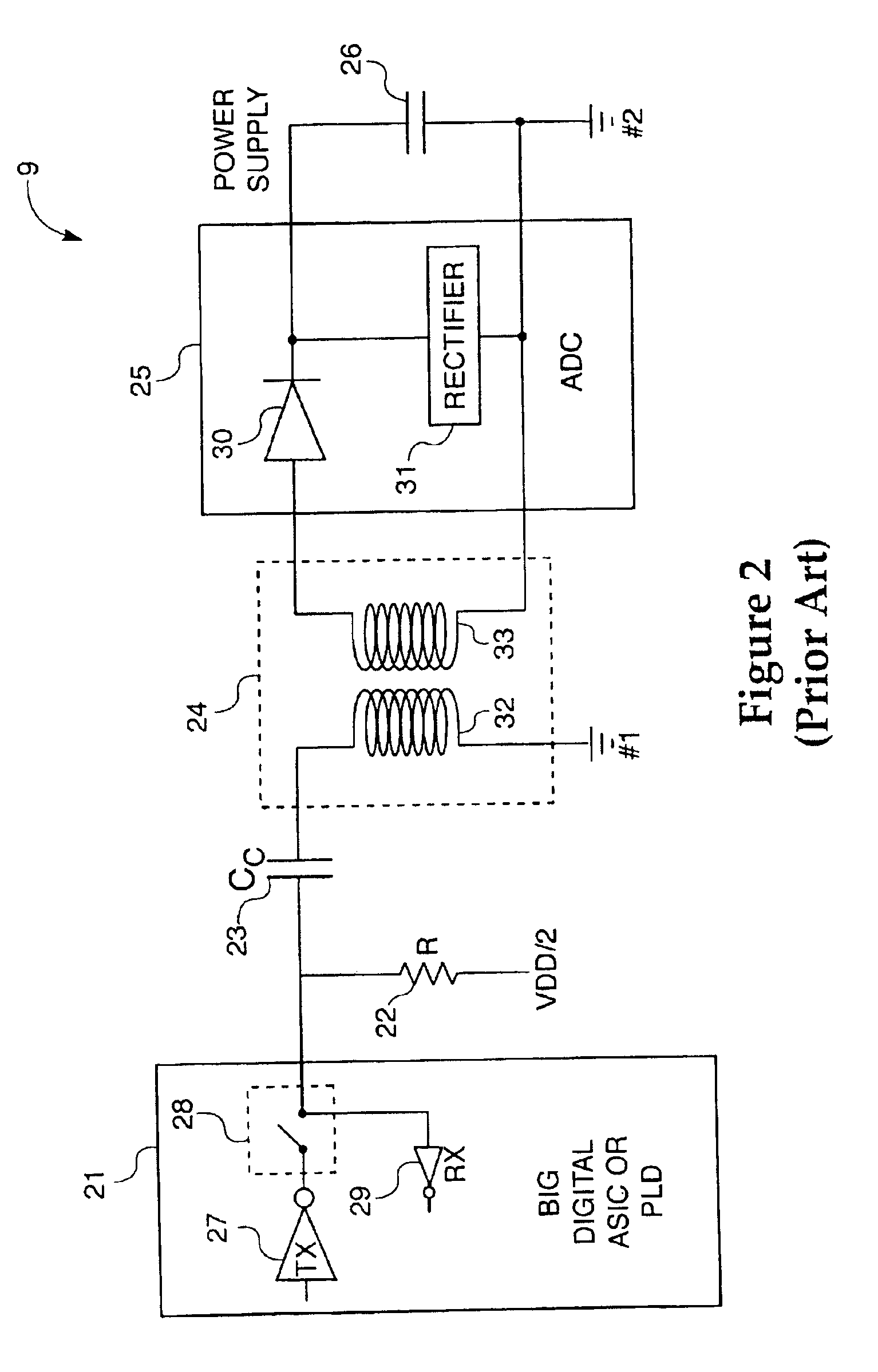
During this take-over period, however, voltage at power supply 26 may droop significantly if many bits are transmitted, and full logic levels may not re-establish themselves.
CMOS circuitry may be more susceptible to drift due to temperature variations and the like, as well as initial accuracy of measurement.
However, such as solution creates extra cost and increases complexity and size of the overall circuitry.

Method used


Image

  • Calibration of isolated analog-to-digital converters
  • Calibration of isolated analog-to-digital converters
  • Calibration of isolated analog-to-digital converters

Examples


Embodiment Construction

[0029]Referring now to FIG. 3, there is known a block diagram of a two channel isolated analog-to-digital converter system 139, wherein the analog-to-digital converter 143 and 153 are isolated from the microprocessor or programmable logic device 141 by first and second transformers 142 and 152, respectively.

[0030]System 139 includes a microprocessor or programmable logic device 141 which is coupled to first and second analog-to-digital converters 143 and 153 through respective first and second transformers 142 and 152. A current limiting / isolating resistor RL 145 may limit overall current and isolate the two calibration resistors R1, 144 and R2 146 from one another. First and second calibration resistors R1 144 and R2 146 may be coupled to the outputs of analog-to-digital converters 143, and 153, respectively.

[0031]First and second analog-to-digital converters 143, and 153 may be referenced to respective local grounds GND1 and GND2, which may be at very different potentials. In norm...


PUM


Abstract

Measurement data collected by isolated ADCs in multiple channels may be related. In such a scenario, data may be transmitted to a microcontroller or programmable logic device for centralized processing. Gain and offset of the ADCs in different channels, particularly their drift relative to one another, is an issue which requires attention. In particular, a pair of precision resistors is provided in calibrate the different channels. The ADCs may be factory calibrated and the ratio between the two precision resistors stored within the ADCs. The ADCs may later self-calibrate by comparing their relative gains to the stored resistor ratio. Gain of one of the ADCs may be adjusted relative to the other in order to maintain a relative gain calibration. Although absolute gain is not calibrated (as the resistors are isolated) for particular applications, only relative gain between the ADCs is relevant.

Description

CROSS-REFERENCE TO RELATED APPLICATIONS[0001]The present application in a Reissue Application of U.S. patent application Ser. No. 09 / 902,712, now U.S. Pat. No. 6,445,315. The present application contains subject matter related to that in copending U.S. patent application Ser. No. 09 / 834,630, filed on Apr. 16, 2001, entitled “CAPACITIVELY COUPLED REFERENCES FOR ISOLATED ANALOG-TO-DIGITAL CONVERTER SYSTEMS” and U.S. patent application Ser. No. 09 / 690,981, filed Oct. 18, 2000, entitled “Providing Power, Clock and Control Signals as a Single Combined Signal Across an Isolation Barrier in an ADC”, both of which are incorporated herein by reference.FIELD OF THE INVENTION[0002]The present invention relates to analog-to-digital converters. In particular, the present invention is directed toward calibration of isolated analog-to-digital converters.BACKGROUND OF THE INVENTION[0003]Measurement data collected by isolated analog-to-digital converters (ADCs) in multiple data channels may be relat...

Claims


Application Information

Patent Timeline
IPC IPC(8): H03M1/06H03M1/10H03M1/12
CPCH03M1/0827H03M1/1028H03M1/12
Inventor DEN BREEJEN, FRANK
Owner CIRRUS LOGIC INC
Learn More