
TFT LCD device having multi-layered pixel electrodes

Inactive Publication Date: 2010-11-16
SAMSUNG DISPLAY CO LTD
View PDF34 Cites 3 Cited by
  • Summary
  • Abstract
  • Description
  • Claims
  • Application Information

AI Technical Summary

Benefits of technology

[0010]It is an object of the present invention to provide an improved TFT LCD device that can prevent battery effect at the interface between pixel electrodes and drain electrodes, while maintaining high reflectance and conductivity.
[0011]It is another object of the present invention to provide an improved TFT LCD device that can prevent insulating oxides at the interface between pixel electrodes and drain electrodes, while maintaining high reflectance and conductivity.
[0012]It is other object of the present invention to provide an improved TFT LCD device that can prevent contact resistance increase at the interface between pixel electrodes and drain electrodes, while maintaining high reflectance and conductivity.
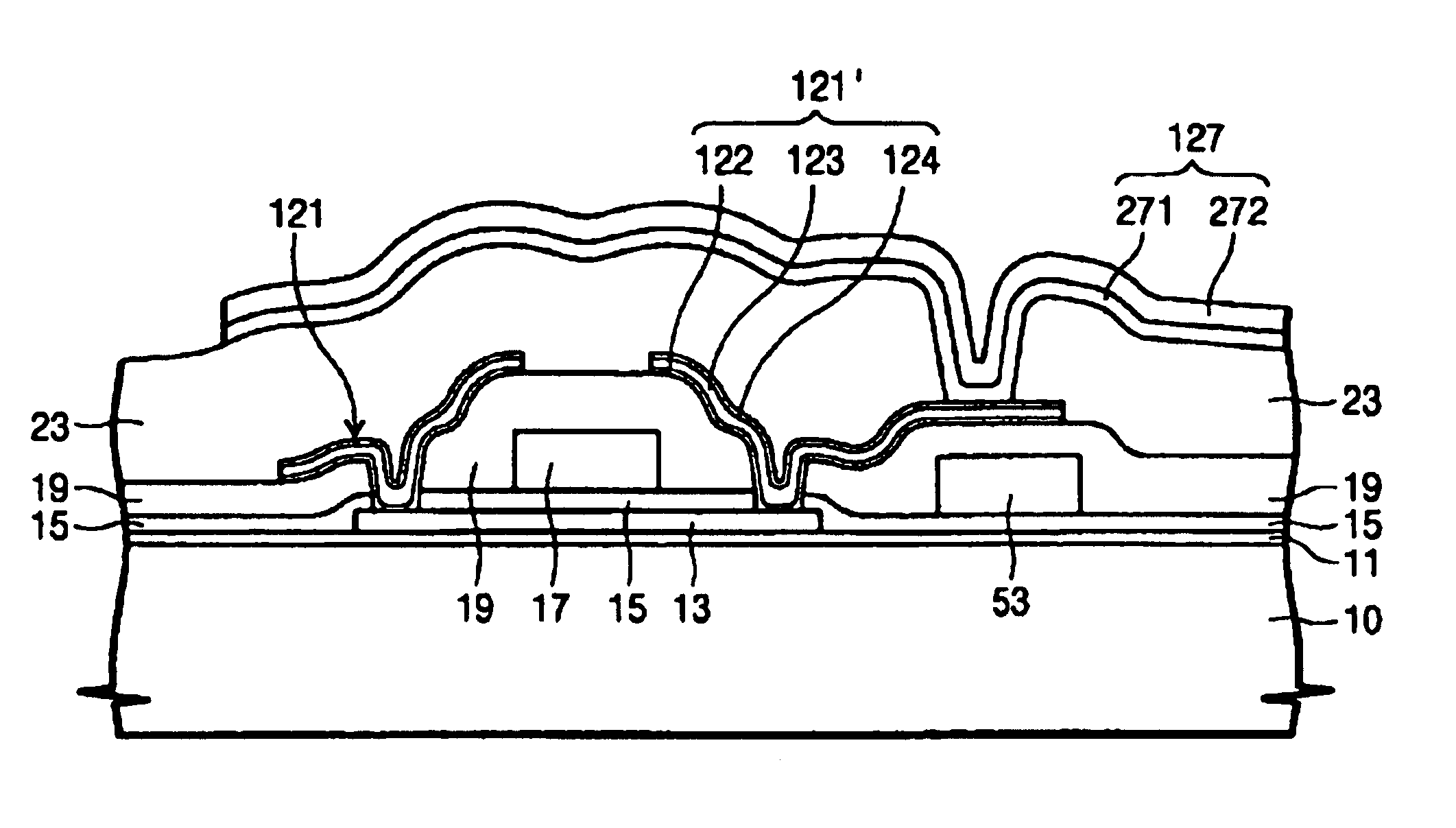
[0015]It is noted that the multi-layered conductive layer is not limited to the two-layered conductive layer. To reduce the battery effect efficiently, if necessary, an intermediate metal layer can be interposed between the lower and upper layers of the two-layered conductive layer.
[0016]The multiple layers of the drain electrodes usually use metal having a high conductivity to prevent a signal voltage drop due to the data line resistance. Also, the drain electrodes are formed of the same conductive material as that of the data lines connected to source electrodes. Accordingly, the multiple layers forming the drain electrodes are preferably composed of a two-layered layer having an Al layer for increasing conductivity and a Cr or MoW layer strongly resistant to oxidation formed on the Al layer, or a three-layered layer having an intermediate Al layer and an upper and a lower Cr or MoW layers formed on and under the intermediate Al-contained layer to prevent spike phenomenon due to silicon layers over an active area. When the drain electrodes formed along with the data lines are of the three-layered layer, the MoW layer as the lower and upper layer preferably is better than the Cr layer since it is easy to be patterned along with the intermediate Al-containing layer.
[0017]According to the present invention, since the upper layer of the drain electrodes and the lower layer of the pixel electrodes are formed of same material or metals having small differences in electro-negativity, the battery effect therebetween can be ignored. Also, in the two-layered conductive layer of the pixel electrodes, the upper layer and the lower layer are concurrently formed to have the same surface area by means of same patterning process. This may result in difference in electro-negativity, but battery effect can be prevented. Thus, at the interface between the pixel electrodes and the drain electrodes, the battery effect is considerably reduced and the spike phenomenon or cracks is prevented.

Problems solved by technology

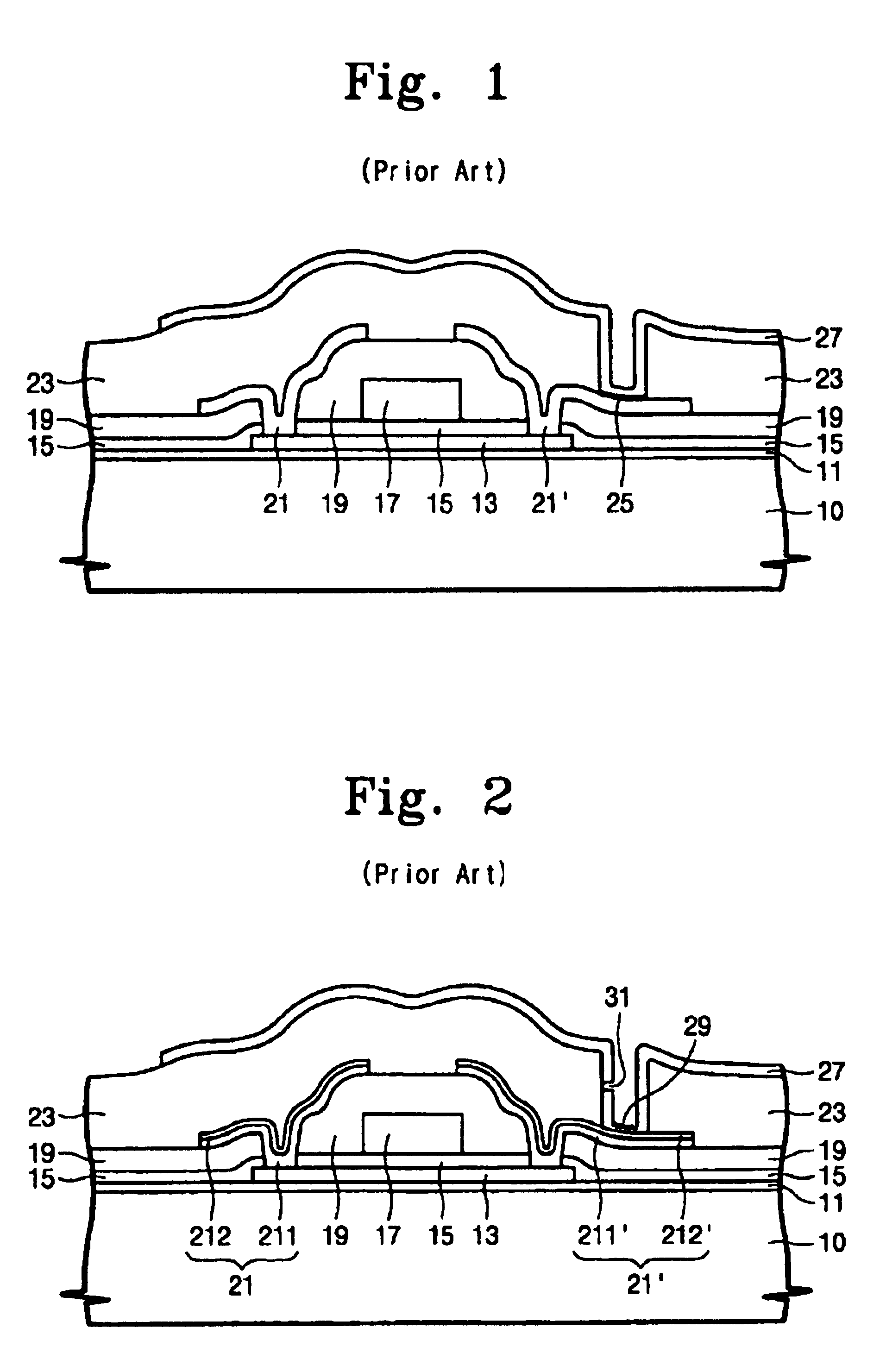
However, this material may cause a problem that oxidizes wires of aluminum (Al) to form insulating oxides and thereby hinders in supplying voltage to the pixel electrodes.
In this case, materials forming drain electrodes are also limited.
However, such a choice deteriorates reflectance and conductivity of the pixel electrodes.

Method used


Image

  • TFT LCD device having multi-layered pixel electrodes
  • TFT LCD device having multi-layered pixel electrodes
  • TFT LCD device having multi-layered pixel electrodes

Examples


Embodiment Construction

[0023]The present invention now will be described more fully hereinafter with reference to the accompanying drawings, in which a preferred embodiment of the invention is shown. This invention may, however, be embodied in many different forms and should not be construed as limited to the embodiment set forth herein. Like numbers refer to like elements throughout.

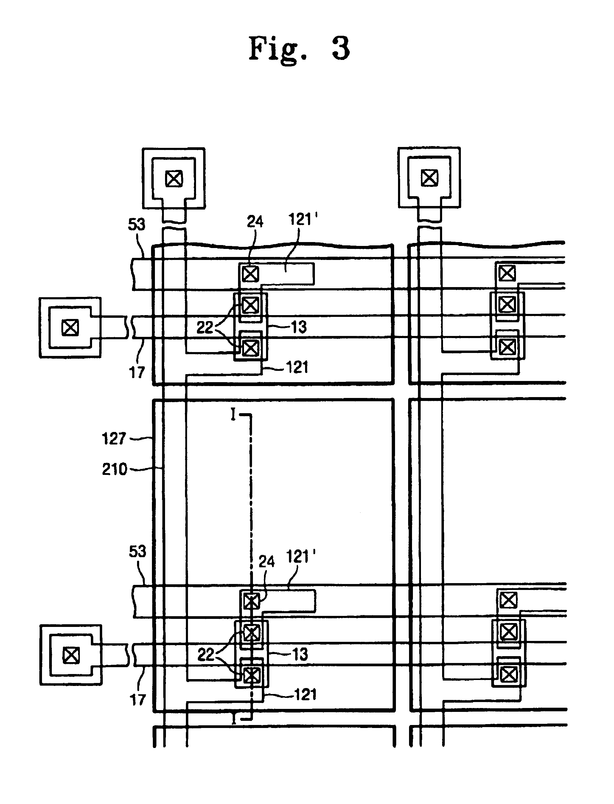
[0024]FIG. 3 is a top plan view showing a layout of pixel portions of a top gate type polysilicon TFT LCD device in accordance with one embodiment of the present invention. Referring to FIG. 3, it can be appreciated that in the top plan view, the pixel portions of the TFT LCD device of the present invention has the same structure as a general reflective or transmissive TFT LCD device. Namely, the TFT LCD device has an active region pattern 13 formed on a substrate, a gate insulating layer (15 of FIG. 4) formed on the active region pattern 13, and thin film transistors formed on the gate insulating layer 15. The thin film tran...


PUM


Abstract

In a TFT LCD device comprising a substrate, at least one thin film transistor formed on the substrate, having a source electrode and a drain electrode, an insulating layer formed over the whole surface of the substrate on which the thin film transistor is formed, having at least one contact hole exposing a portion of the drain electrode, and reflective layer pixel electrode corresponding to the thin film transistor, formed on the insulating layer to be connected with the drain electrode through the contact hole, the pixel electrode is formed of a multi-layered conductive layer. The drain electrode is composed of multiple layers, and the most upper layer of the multiple layers is one selected from a Cr layer and a MoW layer. Preferably, the multi-layered conductive layer is composed of two-layered conductive layer having a lower layer of the same material as that of the most upper layer and an upper layer of Al-containing metal.

Description

CROSS REFERENCE TO PRIOR APPLICATIONS[0001]This application is a reissue application from U.S. patent application Ser. No. 09 / 911,613 filed on Jul. 25, 2001 and issued as U.S. Pat. No. 6,836,299, which claims priority to and the benefit of Korean Patent Application No. 2001-06820 filed on Feb. 12, 2001, which are all hereby incorporated by reference for all purposes as if fully set forth herein. <?insert-end id="INS-S-00001" ?>FIELD OF THE INVENTION[0002]The present invention relates to a thin film transistor liquid crystal display (TFT LCD) device, and more particularly to a reflective or transflective TFT LCD device having multi-layered pixel electrodes connected to drain electrodes with interposing an insulating layer therebetween.BACKGROUND OF THE INVENTION[0003]TFT LCD devices are generally classified into a reflective TFT LCD device using a reflective layer as pixel electrodes, a transmissive TFT LCD device using transparent pixel electrodes, and a transflective TFT LCD ...

Claims


Application Information

Patent Timeline
IPC IPC(8): G02F1/136G02F1/1333G02F1/1343G02F1/1362G02F1/1368H01L21/28H01L21/3205H01L21/336H01L23/52H01L29/786
CPCG02F1/13439G02F1/136227G02F1/1368G02F2203/02H01L29/458H01L27/124G02F1/136
Inventor CHUNG, WOO-SUKHWANG, CHANG-WON
Owner SAMSUNG DISPLAY CO LTD
Learn More