Eureka AIR delivers breakthrough ideas for toughest innovation challenges, trusted by R&D personnel around the world.

Application of reduced dark current photodetector

Active Publication Date: 2021-07-13
MAIMON SHIMON
View PDF40 Cites 0 Cited by
  • Summary
  • Abstract
  • Description
  • Claims
  • Application Information

AI Technical Summary

Benefits of technology

The present invention relates to a photo-detector with reduced dark current and without a depletion layer. The detector comprises a photo absorbing layer, a barrier layer with a significant energy gap to prevent thermalized carriers from flowing to the contact area, and a contact area adjacent to the barrier layer for detecting photons. The detector can be produced without the need for passivation. The technical effect of the invention is to achieve efficient detection of photons with reduced dark current and improved performance.

Problems solved by technology

Highly accurate thermal detectors have been produced using InSb and HgCdTe p-n junction diodes, however these thermal detectors require cooling to cryogenic temperatures of around 77 K which is costly.
The fluctuations of the dark current components are a major factor in the noise that limits the device performance.
Unfortunately this is often difficult to achieve and significantly adds to the cost of production.

Method used


Image

  • Application of reduced dark current photodetector
  • Application of reduced dark current photodetector
  • Application of reduced dark current photodetector

Examples


Embodiment Construction

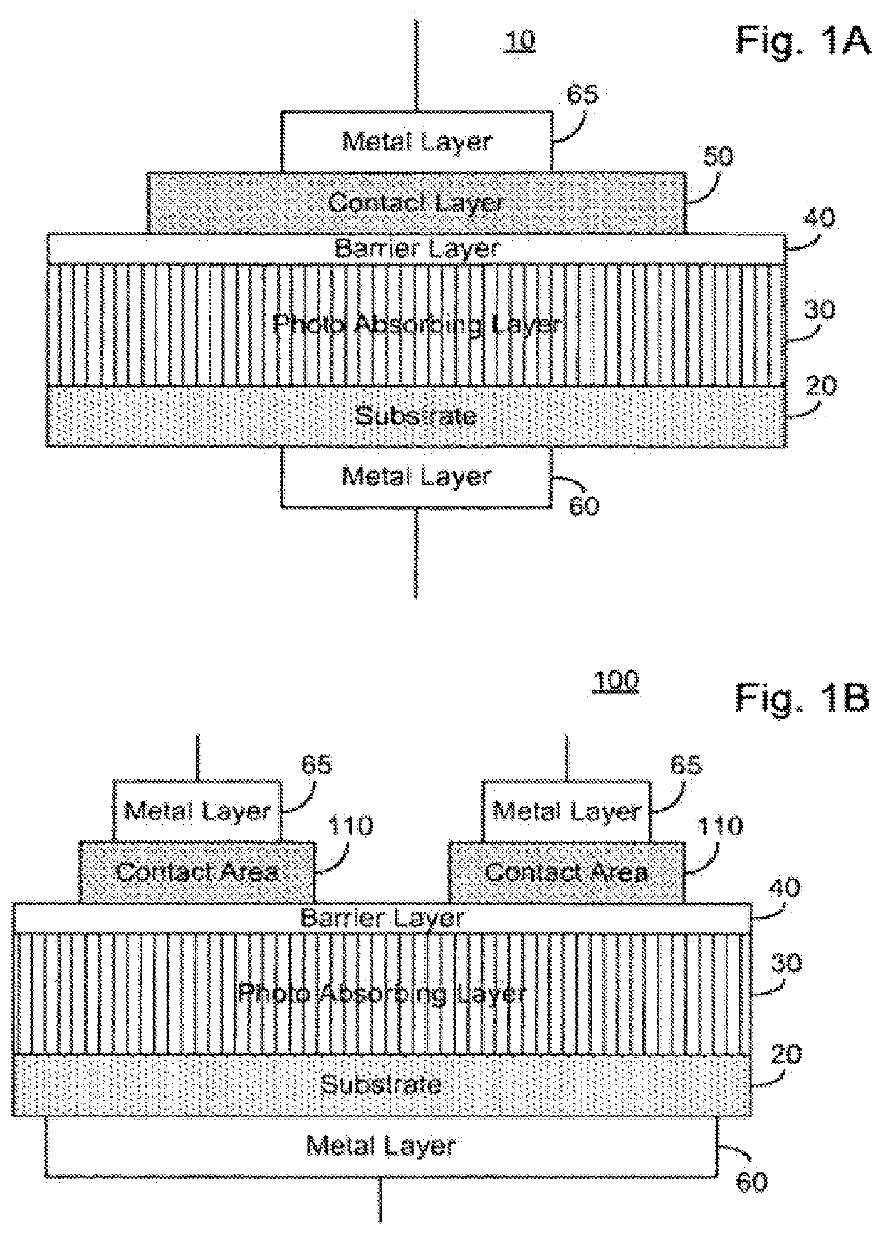
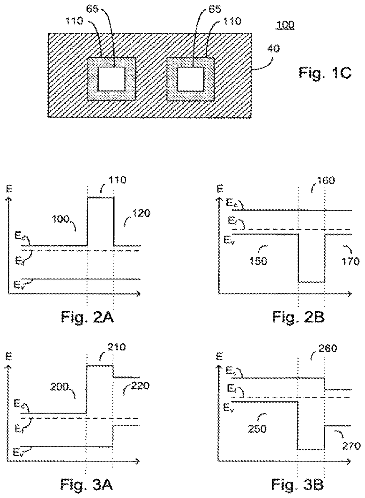
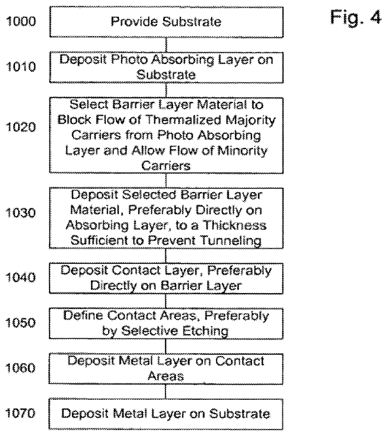
[0053]The present embodiments enable a photo-detector sensitive to a target waveband comprising a photo absorbing layer, preferably exhibiting a thickness on the order of an optical absorption length of the target waveband. In an exemplary embodiment the photo absorbing layer is deposited to a thickness of between one and two times the optical absorption length. A contact layer is further provided, and a barrier layer is interposed between the photo absorbing layer and the contact layer. The barrier layer exhibits a thickness sufficient to prevent tunneling of majority carriers from the photo absorbing layer to the contact layer, and a band gap barrier sufficient to block the flow of thermalized majority carriers from the photo absorbing layer to the contact layer. The barrier layer does not significantly block minority carriers.

[0054]An infra-red detector in accordance with the principle of the invention can be produced using either an n-doped photo absorbing layer or a p-doped pho...


PUM


Abstract

A IDCA system with internal nBn photo-detector comprising: a photo-absorbing layer comprising an n-doped semiconductor exhibiting valence band energy level; a barrier layer, a first side of the barrier layer adjacent a first side of the photo-absorbing layer, the barrier layer exhibiting a valence band energy level substantially equal to the valence band energy level of the doped semiconductor of the photo absorbing layer; and a contact area comprising a doped semiconductor, the contact area being adjacent a second side of the barrier layer opposing the first side, the barrier layer exhibiting a thickness and conductance band gap sufficient to prevent tunneling of majority carriers from the photo-absorbing layer to the contact area, blocking the flow of thermalized majority carriers from the photo-absorbing layer to the contact area. Alternatively, a p-doped semiconductor is utilized, equalizing barrier conductance band energy levels and photo-absorbing layers.

Description

CROSS-REFERENCE TO RELATED APPLICATIONS[0001]This application is a continuation-in-part application of U.S. patent application Ser. No. 13 / 167,992 which was filed on Jun. 24, 2011, which in turn is a continuation of, and claims priority of U.S. patent application Ser. No. 12 / 656,739 filed Feb. 16, 2010, and which in turn is a continuation of, and claims priority of U.S. patent application Ser. No. 11 / 276,962 filed Mar. 19, 2006.This application is a Reissue of U.S. Pat. No. 9,117,726, issued Aug. 25, 2015 on application Ser. No. 13 / 964,883, filed Aug. 12, 2013; which is in turn a continuation-in-part of patent application Ser. No. 13 / 167,992 filed on Jun. 24, 2011 now abandoned; which is in turn a continuation of patent application Ser. No. 12 / 656,739 filed Feb. 16, 2010, issued as U.S. Pat. No. 8,003,434 on Aug. 23, 2011; and which in turn is a divisional of patent application Ser. No. 11 / 276,962 filed Mar. 19, 2006, issued as U.S. Pat. No. 7,687,871 on Mar. 30, 2010. The entire co...

Claims


Application Information

Patent Timeline
IPC IPC(8): H01L27/146H01L23/34G01J5/06
CPCH01L23/34G01J5/061H01L27/14669H01L2924/00H01L2924/0002B82Y20/00G01J2005/0077H01L31/02966H01L31/03046H01L31/035236H01L31/101H01L31/1832H01L31/1844Y02P70/50
Inventor MAIMON, SHIMON
Owner MAIMON SHIMON
Why Eureka
Eureka Blog
Learn More