Manufacturing method of gate pole structure with metal layer lateral surface part removed

A manufacturing method and metal layer technology, applied in semiconductor/solid-state device manufacturing, electrical components, semiconductor devices, etc., can solve problems such as insulation degradation and electrical adverse effects of the overall structure

Inactive Publication Date: 2007-11-28
NAN YA TECH
View PDF6 Cites 0 Cited by
  • Summary
  • Abstract
  • Description
  • Claims
  • Application Information

AI Technical Summary

Problems solved by technology

[0004] Although this method can improve the short circuit problem, because the parts on both sides of the gate metal layer 13 are removed, the insulating layer 15 and the barrier layer 16 will form an arc-shaped part concave to the side of the metal layer 13, thereby making the insulation between the gate electrodes When the layer 17 is formed, the holes 171 shown in Figure 1 will be generated, which will deteriorate the insulation and adversely affect the electrical properties of the overall structure

Method used


Image

  • Manufacturing method of gate pole structure with metal layer lateral surface part removed
  • Manufacturing method of gate pole structure with metal layer lateral surface part removed
  • Manufacturing method of gate pole structure with metal layer lateral surface part removed

Examples


Embodiment Construction

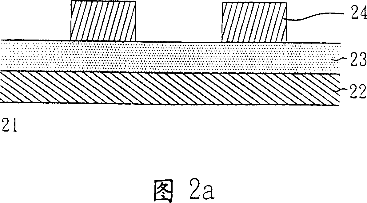
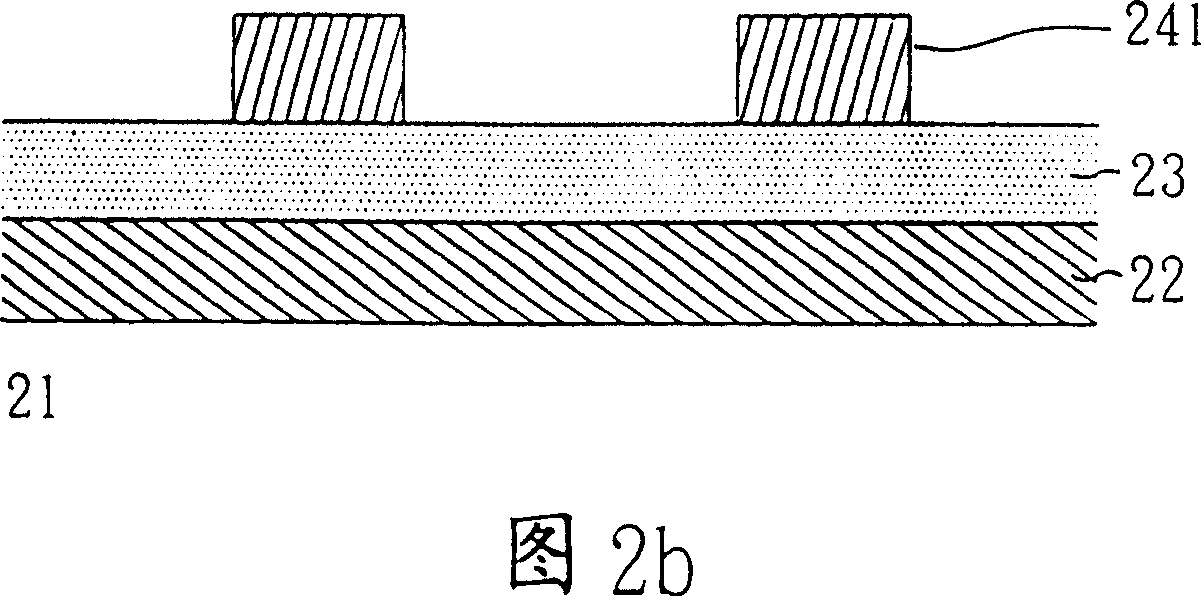
[0026] The schematic cross-sectional views of each step of the method according to the present invention shown in FIGS. 2a to 2g are further described in detail below.

[0027] In FIG. 2a, a conductive layer 22 usually made of polysilicon (Poly-Si) is formed on a substrate 21 usually made of silicon by, for example, deposition, and a conductive layer 22 usually made of tungsten silicide (WSi) is formed on the conductive layer 22 by, for example, deposited. The formed metal layer 23 is formed on the metal layer 23 by, for example, depositing and etching a protective layer 24 usually made of silicon nitride (SiN) with a predetermined gate pattern, wherein each gate pattern has an exposed top surface and side surface .

[0028] Then, the top surface and the side surface of the protection layer 24 can be partially removed by wet etching to form a gate protection layer 241. As shown in FIG. 2b, the removed side surface is preferably less than 20%. Reduce the impact on the gate ele...


PUM


Abstract

A method for making gate structure contains providing a silicon substrate, forming conductive layer on silicon substrate, forming metal layer on conductive layer, forming the per-patterned first protective layer on metal layer wherein every gate pattern has exposed top and side surface, removing part of side surface to form first gate assembly, transferring the pattern of first gate assembly to metal layer to form the second gate assembly, on the substrate, the exposed of first and second gate assembly forming the second protective layer, transferring the first gate assembly and pattern of second gate assembly to conductive layer to form third gate assembly. Said invention ca avoid the improper short circuit between bit line metal layer and gate metal layer without generating cavity in insulation layer between gates.

Description

【Technical field】 [0001] The present invention relates to a method for manufacturing a semiconductor memory, and more specifically, relates to a method for manufacturing a gate structure of a semiconductor memory. 【Background technique】 [0002] In the traditional semiconductor memory manufacturing process, the contact structure is often formed through the contact window, so that the relevant components can achieve the necessary electrical connection. As shown in FIG. 1, the bit line contact structure formed by, for example, the DRAM semiconductor memory manufacturing process mainly includes: a substrate 11 usually made of silicon, a conductive layer 12 usually made of polysilicon (Poly-Si), usually made of tungsten silicide ( Metal layer 13 made of WSi), protective layer 14 usually made of silicon nitride (SiN), insulating layer 15 usually called spacer (spacer) usually made of silicon nitride, barrier rib usually made of silicon nitride Layer 16, insulating layer 17 usual...

Claims


Application Information

Patent Timeline
Patent Type & Authority Patents(China)
IPC IPC(8): H01L21/28H01L21/8234H01L21/8239
Inventor 管式凡吴国坚
Owner NAN YA TECH
Why Eureka
Try Eureka