Electronic component-use substrate and electronic component
A technology for electronic components and substrates, applied in circuit substrate materials, printed circuit components, components of fixed capacitors, etc., and can solve problems such as unresearched
- Summary
- Abstract
- Description
- Claims
- Application Information
AI Technical Summary
Problems solved by technology
Method used
Image
Examples
experiment example 1
[0178] As the resin material, the materials shown in Table 1-1 and 1-2 were prepared, and the mixed materials obtained by mixing the dielectric material powder and magnetic material powder shown in Table 1-1 and 1-2 in the specified ratio were measured respectively. Dielectric constant ε. The results are shown in Tables 1-1 and 1-2. In addition, the decrease in the dielectric constant when the magnetic material is contained is shown in the table together with the comparative sample. In Table 1-1, a conventional comparative sample with a dielectric material powder content of 50 vol %, and a dielectric material powder content of 60 vol % represent a sample of the present invention. In addition, in Table 1-1, in (ε×μ) 1 / 2 In the calculation of , since the magnetic material powder is not included, μ=1 is used for calculation.
[0179]
[0180]
[0181] As can be seen from Tables 1-1 and 1-2, the maximum content of the dielectric material powder and magnetic material powde...
Embodiment 1
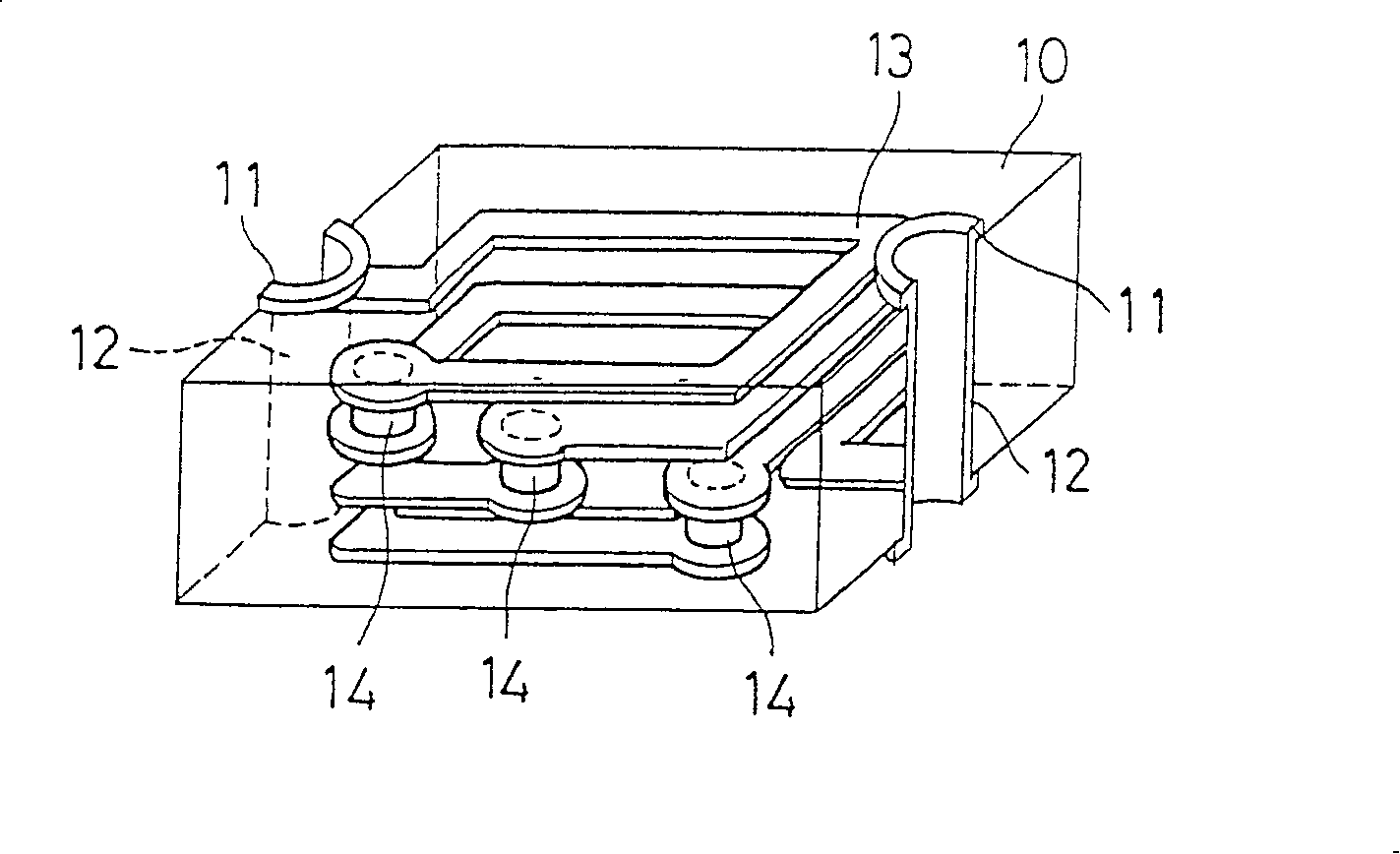
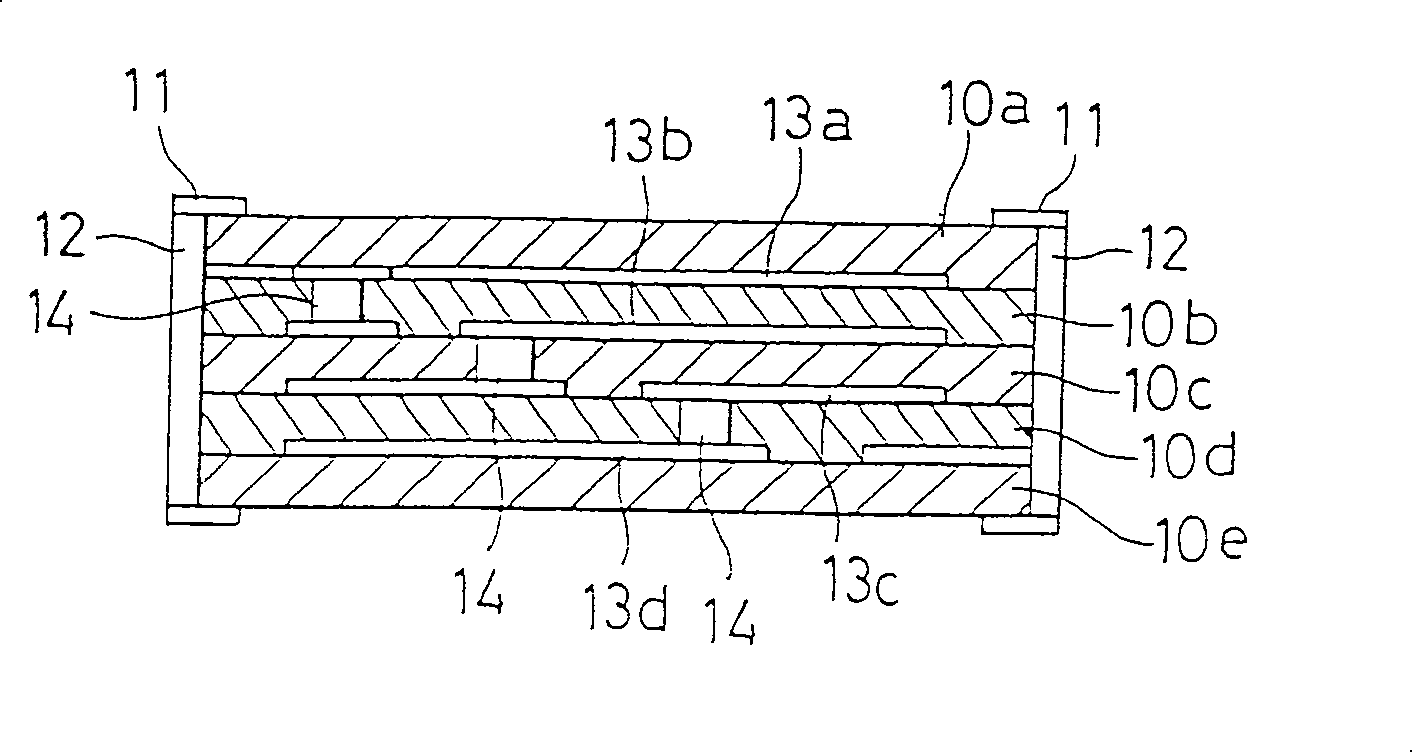
[0183] figure 1 with figure 2 is a diagram showing an inductor as Embodiment 1 of the present invention, figure 1 represents a perspective oblique view, figure 2 Represents a cutaway view.
[0184] In the figure, an inductor 10 includes structural layers (prepreg to substrate) 10a to 10e having the resin of the present invention, internal conductors (coil patterns) 13 formed on process structural layers 10b to 10e, and a coil pattern for the internal conductors. 13 through-holes 14 for electrical connections. The pillar through hole 14 can be formed by drilling, laser processing, etching, or the like. In addition, the terminal wiring of the formed coil is connected to the through-pillar 12 formed on the end surface of the inductor 10 and the terminal pattern 11 formed on the upper and lower sides thereof. The through-pillar 12 is a structure cut in half by cutting, V-cutting, or the like. This is formed by forming a plurality of elements on a collective substrate and c...
Embodiment 2
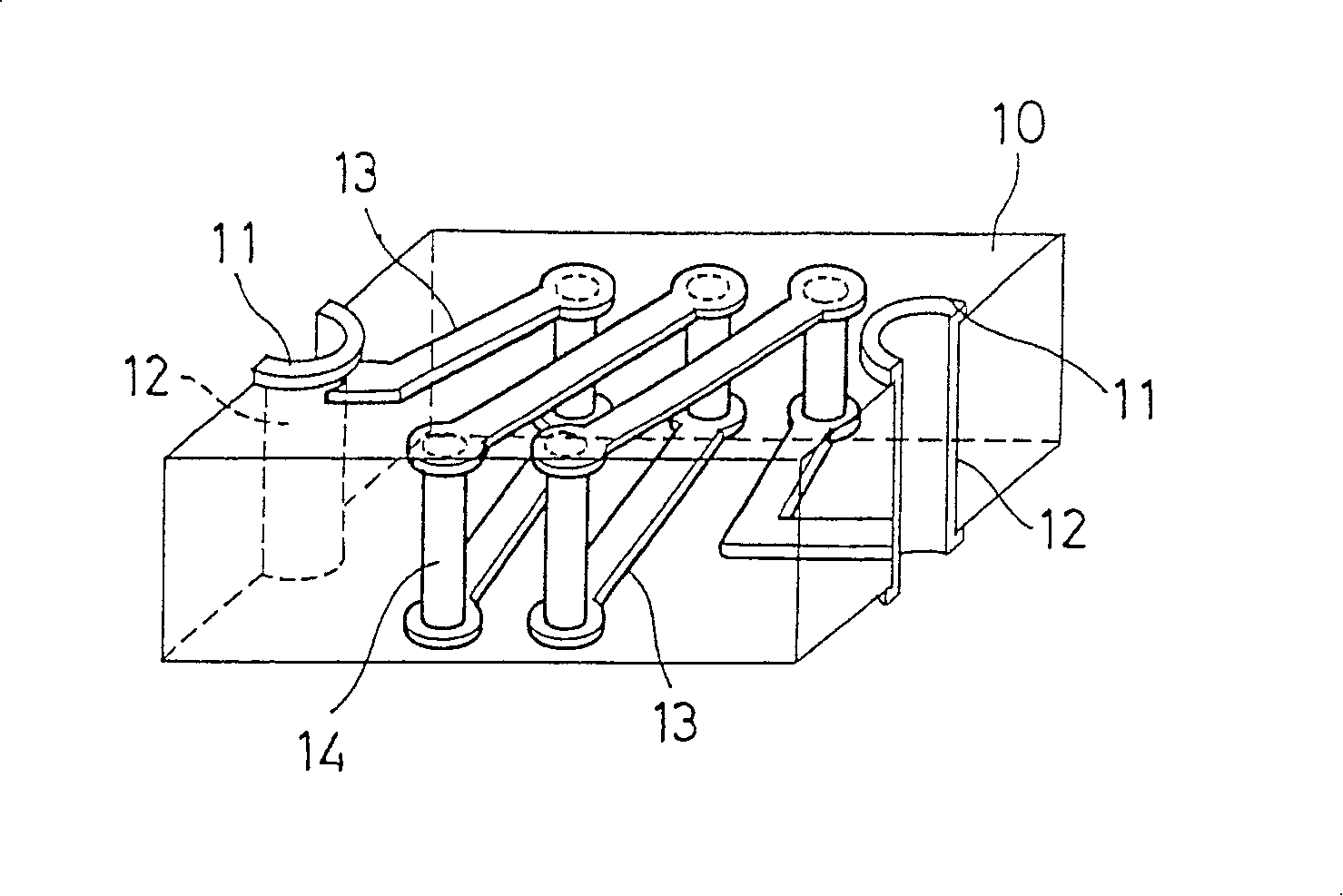
[0189] image 3 with Figure 4 is a diagram showing an inductor as Embodiment 2 of the present invention, image 3 represents a perspective oblique view, Figure 4 Represents a cutaway view.
[0190] In this embodiment, the pattern of the coil wound in the vertical direction in Embodiment 1 is represented as a structural form of a helical coil wound in the lateral direction. The other structural elements are the same as those in Embodiment 1, and the same symbols are assigned to the same structural elements, and description thereof will be omitted.
PUM
| Property | Measurement | Unit |
|---|---|---|
| particle size | aaaaa | aaaaa |
| particle size | aaaaa | aaaaa |
| particle diameter | aaaaa | aaaaa |
Abstract
Description
Claims
Application Information


