Methods for planarization of dielectric layer around metal patterns for optical efficiency enhancement

An image sensor and semiconductor technology, applied in semiconductor devices, semiconductor/solid-state device manufacturing, electrical components, etc., can solve problems such as substrate parallelism, pattern drop, reduced sensor performance, etc., to reduce refraction, eliminate Non-uniform thickness, the effect of improving optical sensitivity

Active Publication Date: 2008-09-17
TAIWAN SEMICON MFG CO LTD
View PDF5 Cites 0 Cited by
  • Summary
  • Abstract
  • Description
  • Claims
  • Application Information

AI Technical Summary

Problems solved by technology

Due to the loading effect of the chemical mechanical polishing process and the non-uniform height of the first dielectric layer 110, the polishing process causes the dielectric material between and above the metal layers 106 and 108 to have a sloped surface that does not contact the substrate. parallel and uneven
The sloping surface of this dielectric layer refers to the non-uniform thickness. Since the non-uniform thickness will cause a drop between the patterns, it will not only cause visible color difference, but also reduce the performance of the sensor. These patterns also include Prisms formed on the dielectric layer and sensing units formed in / on the substrate and under the dielectric layer

Method used


Image

  • Methods for planarization of dielectric layer around metal patterns for optical efficiency enhancement
  • Methods for planarization of dielectric layer around metal patterns for optical efficiency enhancement
  • Methods for planarization of dielectric layer around metal patterns for optical efficiency enhancement

Examples


Embodiment Construction

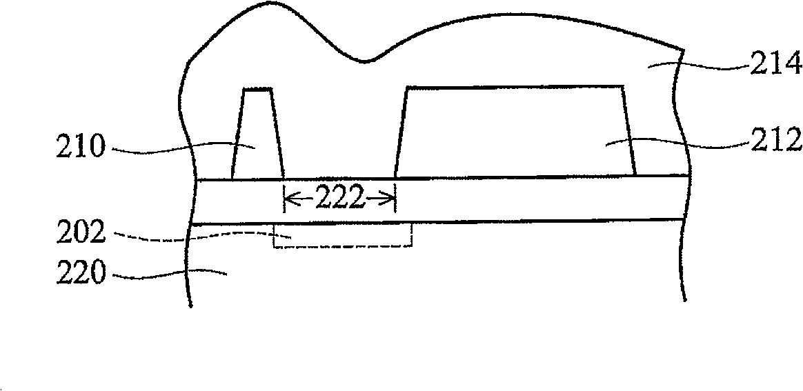
[0022] Please refer to Figure 2A to Figure 2D , which illustrates a manufacturing process for processing a dielectric layer according to a first embodiment of the present invention. This flow shows a method to uniformly planarize the surface of the dielectric layer, which is the four steps described in one embodiment for this purpose.

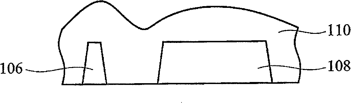
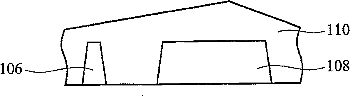
[0023] Please refer to Figure 2A , the metal layers 210 and 212 are used to block electromagnetic radiation in the optical wavelength range, especially light radiation. The metal layers 210 and 212 are metal patterns, and the whole can be formed into a metal pattern, which can be formed by plasma etching. The metal layers 210 and 212 can be lines, islands, or pads composed of metals such as copper, aluminum, various metal compounds, or metal alloys. The metal layers 210 and 212 may be the same metal layer or different metal layers. The metal layers 210 and 212 may also have different sizes, and the heights of the metal layers 210 and 212 m...


PUM

PropertyMeasurementUnit
thicknessaaaaaaaaaa
thicknessaaaaaaaaaa
thicknessaaaaaaaaaa

Abstract

A method and system for improving planarization and uniformity of dielectric layers for providing improved optical efficiency in CCD and CMOS image sensor devices. In various embodiments, a dielectric planarization method for achieving better optical efficiency includes first depositing a first dielectric having an optically transparent property on and around a metal pattern. Optical sensors are formed in or on the substrate in areas between metal features. The metal pattern protects a sensor situated therebetween and thereunder from electromagnetic radiation. After the first dielectric layer is polished using CMP, a slanted or inclined surface is produced but this non-uniformity is eliminated using further planarization processes that produce a uniform total dielectric thickness for the proper functioning of the sensor.

Description

technical field [0001] The present invention relates to semiconductor processing methods, and more particularly, to methods and structures for planarizing dielectric layers around metal patterns to facilitate enhanced optical performance. Background technique [0002] In recent years, the application of optical components such as complementary metal oxide semiconductor (CMOS) image sensors (CCDs) has flourished. Compared with general logic elements, these elements have many special requirements. For example, one of these requirements is to reduce the thickness of the light-transmitting dielectric layer in the protective layer of the back-end process. These dielectric layers are such as silicon dioxide, Silicon nitride, or silicon oxynitride. Another requirement is that the thickness of the light-transmitting dielectric material between each metal pattern should be kept uniform, and the thickness of the dielectric material above the metal pattern should also be kept uniform....

Claims


Application Information

Patent Timeline
Patent Type & Authority Patents(China)
IPC IPC(8): H01L21/00H01L21/3105H01L27/146H01L27/14H01L21/4763H01L21/768
CPCH01L27/14621H01L27/14685H01L27/14627H01L21/76819H01L27/14683
Inventor 谢友岚林志旻王建忠
Owner TAIWAN SEMICON MFG CO LTD
Why Eureka
Try Eureka