
Indium ¿C gallium ¿C arsenic line detectors with micro mesa-structure

A mesa structure, indium gallium arsenic technology, applied in the direction of semiconductor devices, sustainable manufacturing/processing, electrical components, etc., can solve the problems of affecting the detection rate of detectors, unfavorable device performance, increasing the surface recombination of photogenerated carriers, and achieving Improve long-term stability and reliability, and reduce the effect of contact surface states

Inactive Publication Date: 2008-10-08
SHANGHAI INST OF TECHNICAL PHYSICS - CHINESE ACAD OF SCI
View PDF5 Cites 0 Cited by
  • Summary
  • Abstract
  • Description
  • Claims
  • Application Information

AI Technical Summary

Problems solved by technology

During annealing, InP surface will produce In condensation and P vacancies, which will increase the surface recombination of photogenerated carriers and affect the detection rate of the detector, so it will have a negative impact on device performance.

Method used


Image

  • Indium ¿C gallium ¿C arsenic line detectors with micro mesa-structure
  • Indium ¿C gallium ¿C arsenic line detectors with micro mesa-structure
  • Indium ¿C gallium ¿C arsenic line detectors with micro mesa-structure

Examples


Embodiment Construction

[0013] Below in conjunction with accompanying drawing, the specific embodiment of the present invention is described in detail:

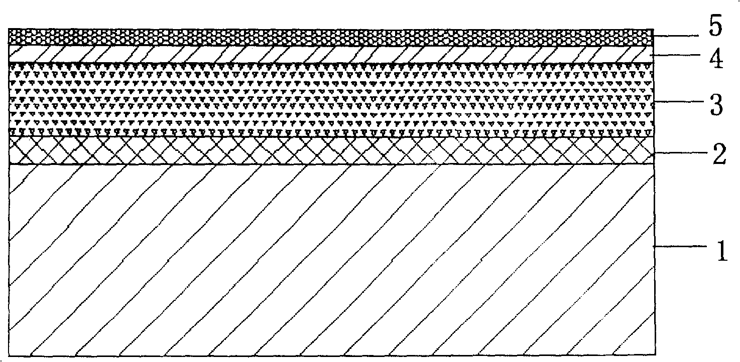
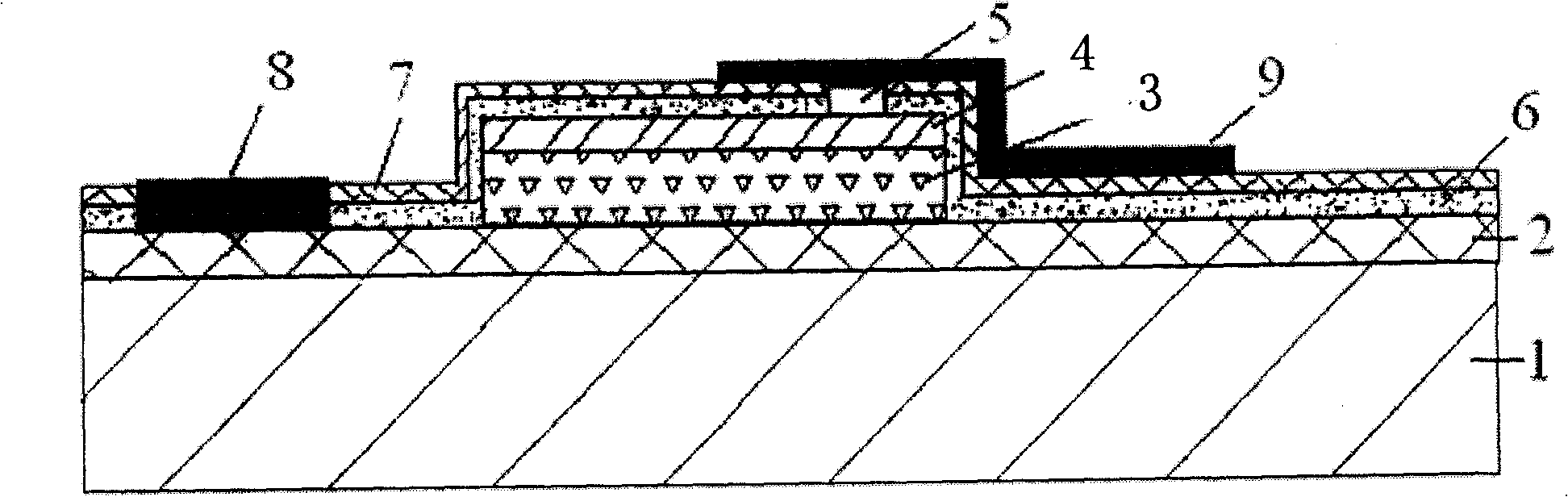
[0014] Such as figure 1 As shown, the epitaxial wafer includes: a semi-insulating InP substrate 1 with a thickness of 500 μm, which is sequentially arranged and grown on the semi-insulating InP substrate with a thickness of 1 μm and a carrier concentration of 2×10 18 cm -3 The n-type InP layer 2; the thickness is 2.5 μm, and the Si-doped concentration is 2×10 16 cm -3 In 0.53 Ga 0.47 As absorption layer 3; the thickness is 0.5 μm, and the carrier concentration is 2×10 18 cm -3 The P-type InP layer 4; the thickness is 20nm, and the carrier concentration is 2×10 18 cm -3 p-InGaAs layer 5.

[0015] The device preparation process is as follows:

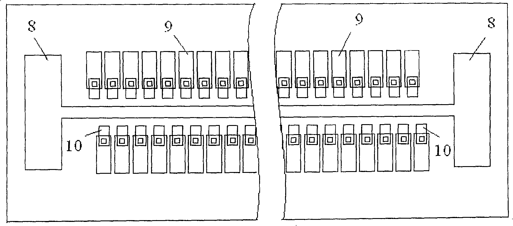
[0016] 1. Ultrasonic cleaning the epitaxial wafer with chloroform, ether, acetone, and ethanol in sequence, each time for more than 2 minutes, and then blowing dry with nitrogen;

[0017] 2. Positive...


PUM


Abstract

Structure of the detector is as following: there is n type InP layer on semi insulated InP substrate; line array micro tabletop formed through etching and composed of InGaAs absorbed layer and p type InP layer is setup on n type InP layer; a layer of p-InGaAs electrode transition layer is developed on leadout area of p type electrode on micro tabletop; In2S3 layer built through sulphidizing process covers all bare areas on the micro tabletop; there are In2S3 passivation layer and SiNx passivation layer made through heat evaporation in sequence on the In2S3 layer. Matched crystal lattice between In2S3 built through sulphidizing process and In2S3 passivation layer reduces contact surface state and dark current, and increases quantum efficiency. SiNx passivation layer raises stability and reliability. P-InGaAs electrode transition layer realizes ohmic contact of Ti / Pt / Au electrodes without anneal. Small contact resistance raises performance of detector.

Description

technical field [0001] The invention relates to an indium gallium arsenic linear detector, in particular to a double-layer passivated indium gallium arsenic linear detector with a micro-mesa structure. Background technique [0002] Since short-wave InGaAs detectors can work at room temperature and have a higher detection rate than HgCdTe detectors, they have broad application prospects in military and civilian fields. [0003] At present, most InGaAs detectors adopt n-InP / i-InGaAs / p-InP epitaxial micro-mesa structure, and anti-reflection passivation film is grown on the upper surface and side of the micro-mesa, and the passivation film is mostly polyimide, SiO 2 、SiN x Wait. Due to SiN x , SiO 2 The thin film does not match the InP and InGaAs lattice, and it is easy to generate stress when the ambient temperature changes, which cannot guarantee the long-term stability of the device; polyimide has corrosion resistance, radiation resistance, high temperature resistance, an...

Claims


Application Information

Patent Timeline
Patent Type & Authority Patents(China)
IPC IPC(8): H01L31/105H01L31/18
CPCY02P70/50
Inventor 吕衍秋韩冰唐恒敬任仁吴小利乔辉张可锋李雪龚海梅
Owner SHANGHAI INST OF TECHNICAL PHYSICS - CHINESE ACAD OF SCI
Features
  • Generate Ideas
  • Intellectual Property
  • Life Sciences
  • Materials
  • Tech Scout
  • Unparalleled Data Quality
  • Higher Quality Content
  • 60% Fewer Hallucinations
Learn More