InGaAs low table face linear array or face array infrared detector chip
An infrared detector and mesa line technology, applied in the field of infrared detectors, can solve the problems of reduced device reliability, complicated diffusion process, enlarged photosensitive surface, etc., and achieve the effect of improving device reliability
- Summary
- Abstract
- Description
- Claims
- Application Information
AI Technical Summary
Problems solved by technology
Method used
Image


Examples
Embodiment Construction
[0013] Below in conjunction with accompanying drawing and embodiment the specific embodiment of the present invention is described in further detail:
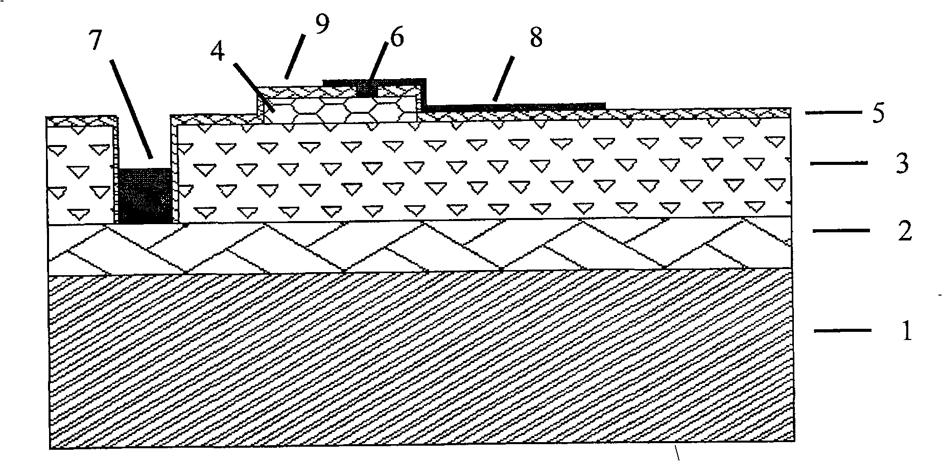
[0014] See figure 1 The epitaxial wafer used in this embodiment is an n-type InP layer 2 with a thickness of 1 μm grown sequentially on a semi-insulating InP substrate 1 with a thickness of 350 μm by MBE technology, and the carrier concentration is greater than 2×10 18 cm -3 ; In with a thickness of 2.5 μm 0.53 Ga 0.47 As intrinsic absorption layer 3; p-type InP cap layer 4 with a thickness of 0.5 μm, and a carrier concentration greater than 2×10 18 cm -3 .
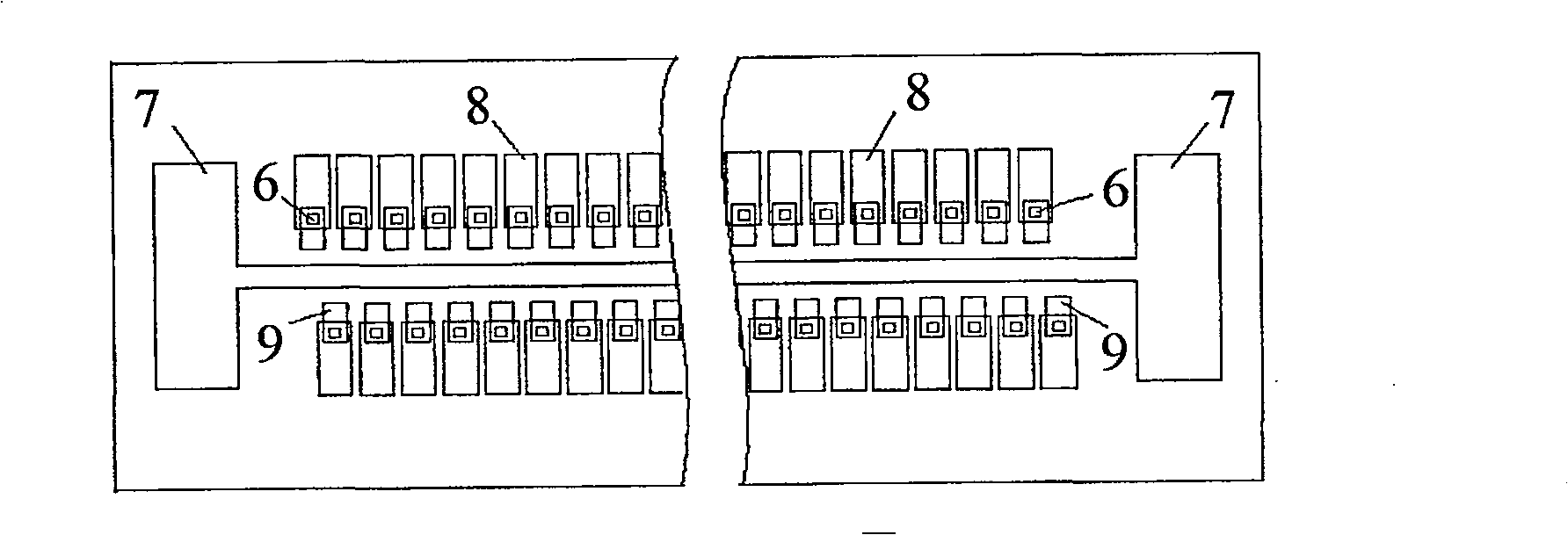
[0015] figure 2 It is a schematic diagram of the cross-sectional structure of this embodiment, and the linear p-InP micro-mesas 4 are formed on the epitaxial wafer by etching. A P electrode region 6 is placed on a local area of the p-InP micro-mesa, and the P electrode in ohmic contact with the p-InP is made of Au / Zn / Pt / Au, and Au, Zn, Pt, and Au are sequentially...
PUM
 Abstract
Description
Claims
Application Information
 - Generate Ideas
- Intellectual Property
- Life Sciences
- Materials
- Tech Scout
- Unparalleled Data Quality
- Higher Quality Content
- 60% Fewer Hallucinations
Browse by: Latest US Patents, China's latest patents, Technical Efficacy Thesaurus, Application Domain, Technology Topic, Popular Technical Reports.
© 2025 PatSnap. All rights reserved.Legal|Privacy policy|Modern Slavery Act Transparency Statement|Sitemap|About US| Contact US: help@patsnap.com