InGaAs low table face linear array or face array infrared detector chip

A technology of infrared detectors and mesa wires, applied in the field of infrared detectors, can solve the problems of device reliability reduction, bad side passivation, limit device detection rate, etc., and achieve the effect of improving device reliability and preventing external diffusion

Active Publication Date: 2008-04-30
SHANGHAI INST OF TECHNICAL PHYSICS - CHINESE ACAD OF SCI
View PDF0 Cites 5 Cited by
  • Summary
  • Abstract
  • Description
  • Claims
  • Application Information

AI Technical Summary

Problems solved by technology

This method can obtain an InGaAs detector with a higher detection rate, but it has some unavoidable disadvantages: the diffusion process is complicated, the photosensitive surface is enlarged, and Zn diffusion will cause a large number of defects in the InP layer, which limits the indium Performance Improvement of GaAs Detectors
The advantage of this structure is that the process is relatively simple, and the disadvantage is that the side exposure of the thicker absorbing layer introduces a large number of interface states, which limits the improvement of the device detection rate to a large extent, and poor side passivation will make the device reliable. decreased sex
In addition, it is also a difficult problem to reliably realize the extraction of ohmic contact electrodes on the p-InP cap layer

Method used


Image

  • InGaAs low table face linear array or face array infrared detector chip
  • InGaAs low table face linear array or face array infrared detector chip
  • InGaAs low table face linear array or face array infrared detector chip

Examples


Embodiment Construction

[0013] Below in conjunction with accompanying drawing and embodiment the specific embodiment of the present invention is described in further detail:

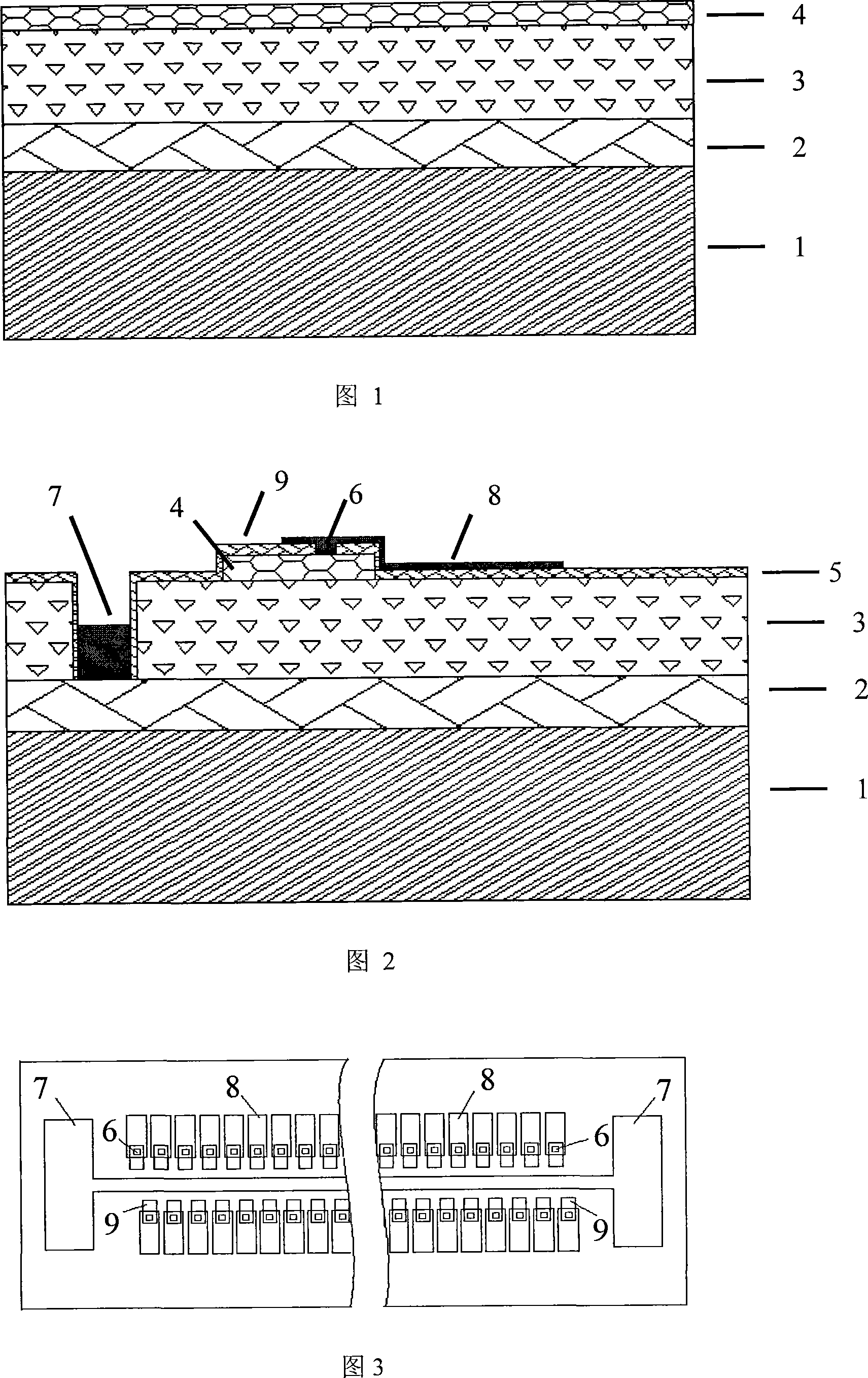
[0014] As shown in Fig. 1, the epitaxial wafer used in this embodiment is an n-type InP layer 2 with a thickness of 1 μm grown sequentially on a semi-insulating InP substrate 1 with a thickness of 350 μm by MBE technology, and the carrier concentration is greater than 2×10 18 cm -3 ; In with a thickness of 2.5 μm 0.53 Ga 0.47 As intrinsic absorption layer 3; p-type InP cap layer 4 with a thickness of 0.5 μm, and a carrier concentration greater than 2×10 18 cm -3 .

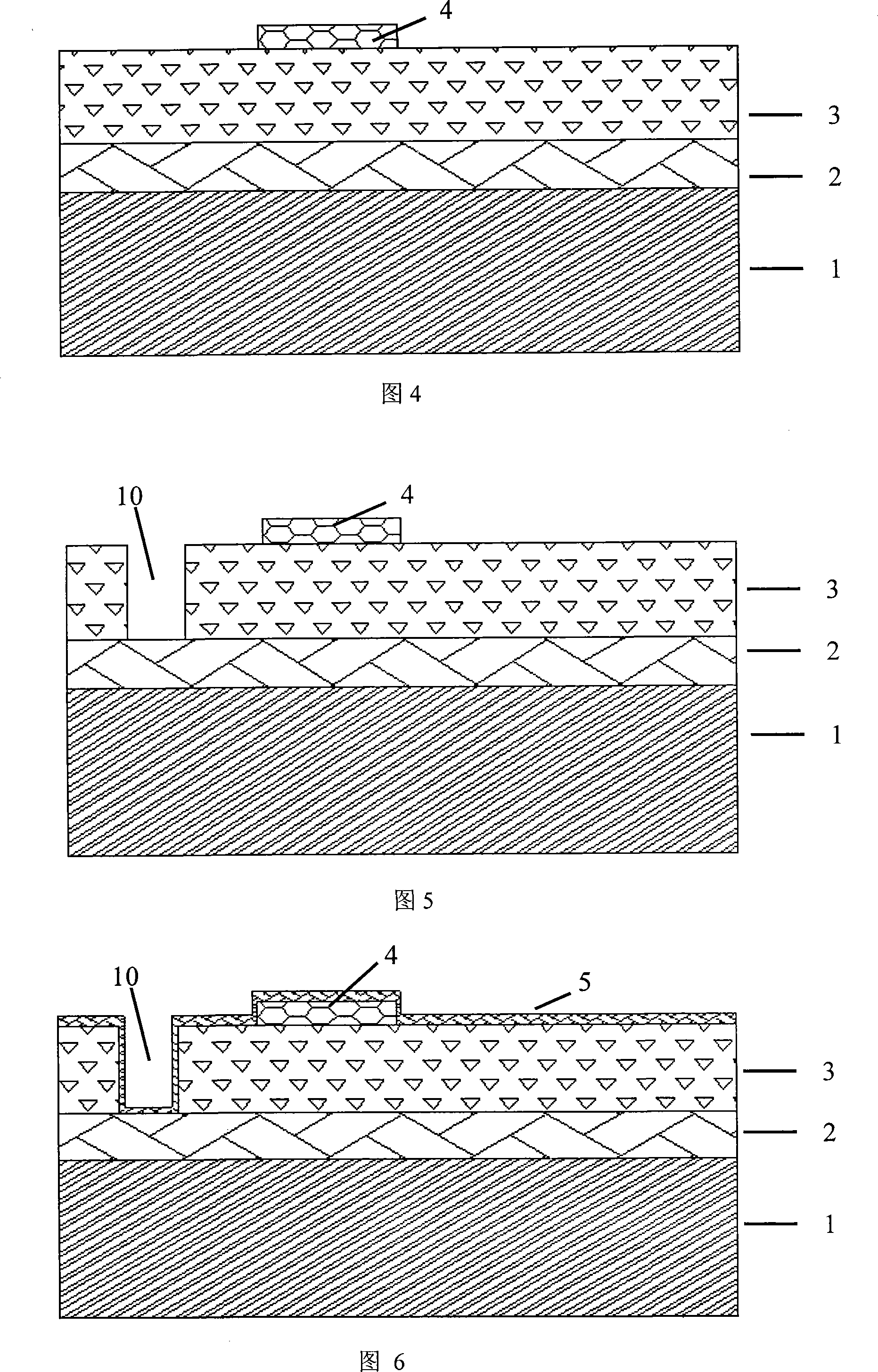
[0015] FIG. 2 is a schematic cross-sectional structure diagram of the present embodiment, in which linear p-InP micro-mesas 4 are formed on the epitaxial wafer by etching. Au / Zn / Pt / Au / P electrode region 6 in ohmic contact with p-InP is placed on the local area of ​​the p-InP micro-mesas, and there is an etching to the n-InP layer on the edge of the line-column ...


PUM


Abstract

The invention discloses an InGaAs low mesa line series or area array infrared detector chip, which includes a line series or area array p-InP micro-mesa formed by etching on p-InP/InGaAs/n-InP epitaxial wafer. The p-InP micro-mesa is provided with an Au/Zn/Pt/Au/P electrode area in ohmic contact. A public N electrode area is etched to the n-InP layer on the side of the line series or area array micro-mesa and is positioned on the n-InP layer. Except for the P and N electrode areas, the whole epitaxial wafer and the lateral sides are covered by a silicon nitride passivation layer. The P electrode area is provided with an electrode interconnection area with a reading circuit. The electrode interconnection area covers a part of the micro-mesa and extends from the micro-mesa to a plane. The invention has the advantages of mesa decrease by retained InGaAs layer and effective protection on the InGaAs layer lateral sides. The silicon nitride passivation layer has effective function of reflection resistance and InP and InGaAs layer surface state reduction and can increase the detector quantum efficiency and decrease dark current. The P electrode adopts AuZnPtAu, forms good ohmic contact with p-InP and P can effectively prevent Zn from out diffusion and improve the device reliability.

Description

technical field [0001] The invention relates to an infrared detector, in particular to a p-InP / InGaAs / n-InP (PIN) low-level line array or area array infrared detector chip. Background technique [0002] At present, PIN InGaAs detectors are mainly divided into two types: planar type and mesa type. Most planar PIN InGaAs detectors use Zn diffusion method to achieve p-type doping in the n-InP / InGaAs / n-InP cap layer InP. This method can obtain an InGaAs detector with a higher detection rate, but it has some unavoidable disadvantages: the diffusion process is complicated, the photosensitive surface is enlarged, and Zn diffusion will cause a large number of defects in the InP layer, which limit the indium GaAs detector performance enhancement. The mesa-type InGaAs detector is to etch the p-InP / InGaAs in the epitaxial material into a mesa, the cap layer p-InP is relatively thin, generally 0.1-0.5 μm, and the InGaAs absorption layer is thick, generally 1.5-3 μm . The advantage o...

Claims


Application Information

Patent Timeline
Patent Type & Authority Applications(China)
IPC IPC(8): H01L31/105H01L31/0224
Inventor 唐恒敬吴小利张可锋汪洋刘向阳李永富吴家荣李雪龚海梅
Owner SHANGHAI INST OF TECHNICAL PHYSICS - CHINESE ACAD OF SCI
Why Eureka
Try Eureka