Chip of overvoltage protector of semiconductor in low capacitance

An overvoltage protector and semiconductor technology, which is applied in the direction of semiconductor devices, semiconductor/solid-state device parts, electric solid-state devices, etc., can solve the problems of square chips producing boundary and edge effects, affecting the transmission efficiency of communication equipment, etc., to achieve overvoltage Good protection effect, increased effective use area, reasonable layout repetition effect

Inactive Publication Date: 2008-10-15
上海晟芯微电子有限公司
View PDF3 Cites 0 Cited by
  • Summary
  • Abstract
  • Description
  • Claims
  • Application Information

AI Technical Summary

Problems solved by technology

For example, the square chip of the semiconductor overvoltage protector produced in the conventional way, but at the same time, it is easy to bring some negative effects on the circuit, such as the square chip will produce boundary and edge effects
[0004] For the semiconductor overvoltage protector chip of communication equipment, its capacitance often affects the transmission efficiency of communication equipment

Method used


Image

  • Chip of overvoltage protector of semiconductor in low capacitance
  • Chip of overvoltage protector of semiconductor in low capacitance
  • Chip of overvoltage protector of semiconductor in low capacitance

Examples


Embodiment Construction

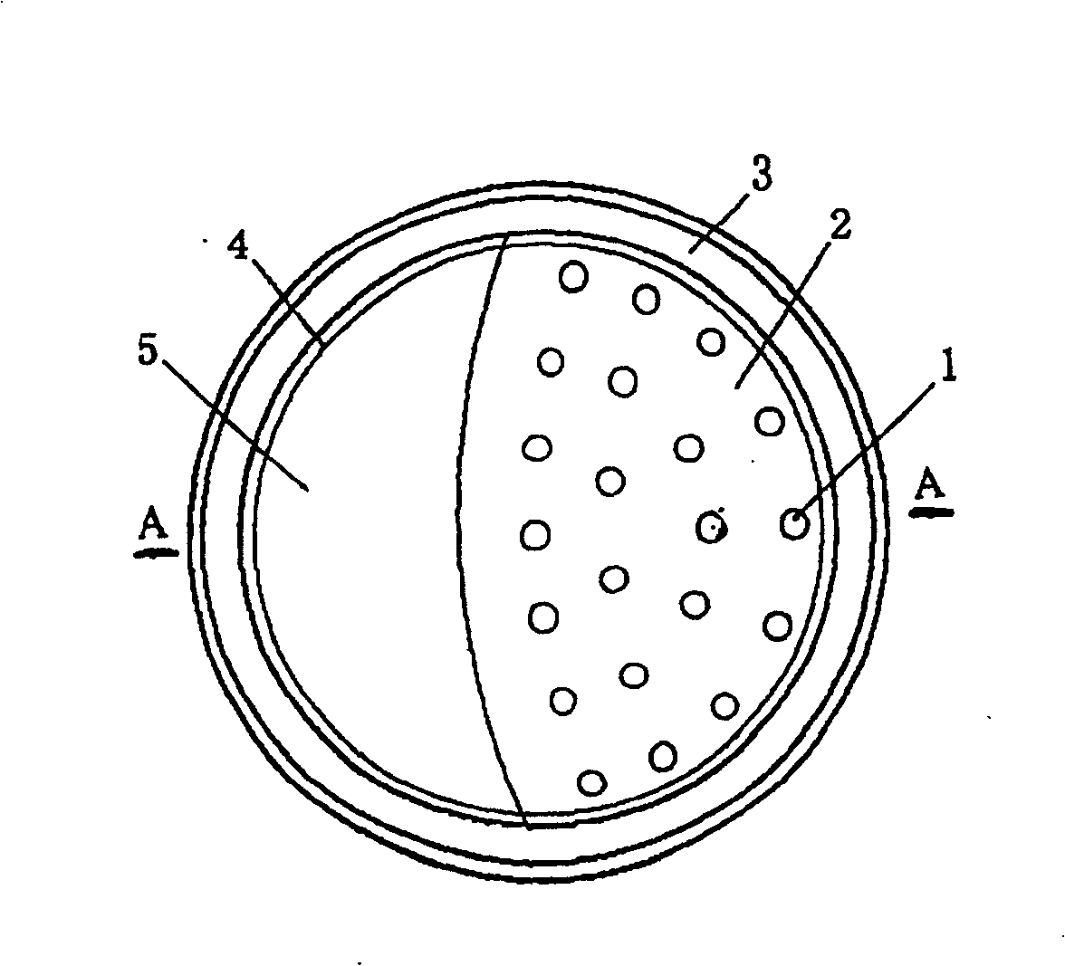
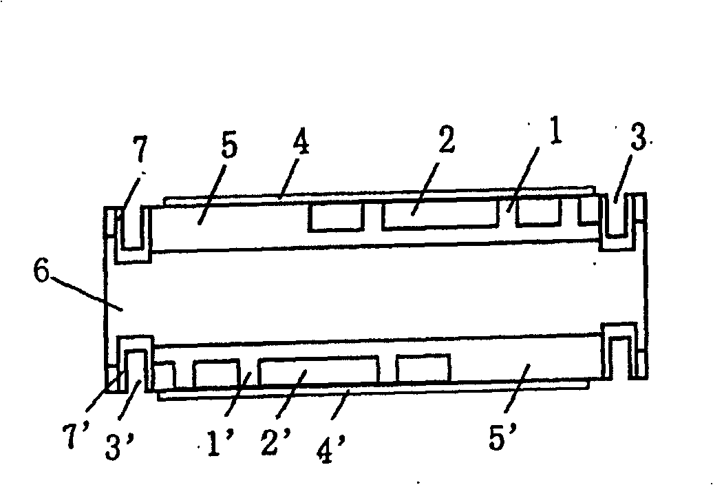
[0013] From figure 1 figure 2 It can be seen that a low-capacitance semiconductor overvoltage protector chip is circular, and the chip includes an N silicon wafer substrate intermediate layer 6, and the upper and lower sides of the N silicon wafer substrate intermediate layer 6 have "base area 5, Emitting area 2, short-circuit point 1" and "base area 5', emitting area 2', short-circuiting point 1'", the upper and lower groups of components are connected to each other and arranged symmetrically. The etched grooves 3 and 3', the inner wall of the etched groove 3 is provided with a glass passivation layer 7, and the surface of the short circuit point 1, the emitter region 2 and the base region 5 is provided with a metal layer 4. A glass passivation layer 7' is placed on the inner sidewall of the etching groove 3', and a metal layer 4' is placed on the surface of the short circuit point 1', the emitter region 2' and the base region 5'.

[0014] The manufacturing process of the ...


PUM


Abstract

The semiconductor chip of overvoltage protector in low capacitance includes intermediate layer on N silicon substrate, as well as base region, emitter region and short dot placed on surface on two sides symmetrical to intermediate layer on N silicon substrate. Characters are that chip is in roundness, and there are etch grooves on peripheries on up and low surfaces of rounded chip. Rounded structural design increases effective area of emitter region, eliminates redundant boron diffusion areas. Thus, the invention possesses relative lower capacitance, satisfies requirement of electrical parameters of circuit, and good effect of overvoltage protection. Moreover, rounded design can increase effective usable floor area on rounded silicon wafer through reasonable repeated composition.

Description

technical field [0001] The invention relates to a semiconductor overvoltage protector, in particular to a chip of a low-capacity semiconductor overvoltage protector used for communication equipment protection. Background technique [0002] Because communication equipment is often exposed to interference from lightning strikes, power line contact, and high-voltage induced electricity, it is very easy to cause irreversible damage to the communication system circuit. Semiconductor overvoltage protectors are often connected in parallel at both ends of the required protection circuit, which can suppress the surge impact generated at both ends of the communication circuit due to the influence of lightning or high-voltage power supply, etc., and realize rapid, economical and stable protection of communication equipment. reliable protection. [0003] Generally speaking, in order to meet the process requirements of mass production of semiconductors, the chip part of semiconductor de...

Claims


Application Information

Patent Timeline
Patent Type & Authority Patents(China)
IPC IPC(8): H01L27/04H01L23/62
Inventor 金国平
Owner 上海晟芯微电子有限公司
Why Eureka
Try Eureka