Transistor structure and control unit having same

A technology for control units and transistors, applied in electrical components, electrical solid-state devices, semiconductor devices, etc., can solve the problems of occupying a considerable circuit area, unfavorable product design and circuit miniaturization.

Active Publication Date: 2008-10-15
AU OPTRONICS CORP
View PDF7 Cites 0 Cited by
  • Summary
  • Abstract
  • Description
  • Claims
  • Application Information

AI Technical Summary

Problems solved by technology

[0006] It can be clearly seen from FIG. 1 that the storage capacitor 12 does have a structure that occupies a considerable lateral portion on the substrate 100. If it is converted to a planar view, it is conceivable that it will inevitably occupy a relatively large circuit area, resulting in restrictions on circuit configuration. , is not conducive to product design and circuit miniaturization

Method used


Image

  • Transistor structure and control unit having same
  • Transistor structure and control unit having same
  • Transistor structure and control unit having same

Examples


Embodiment Construction

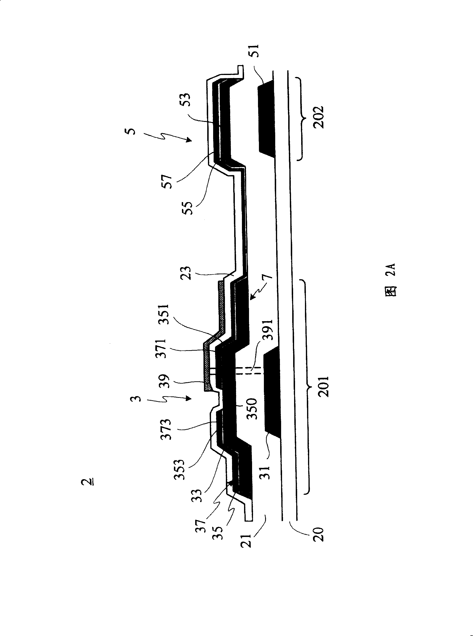
[0042] First please refer to FIG. 2A , which is a schematic cross-sectional view of a control unit 2 according to a preferred embodiment of the present invention; the control unit 2 includes a transistor structure 3 and a first capacitor structure 5 disposed on a substrate 20 . For convenience of description, a control region 201 and a capacitor region 202 can be defined on the substrate 20 , the transistor structure 3 is located on the control region 201 , and the first capacitor structure 5 is located on the capacitor region 202 .

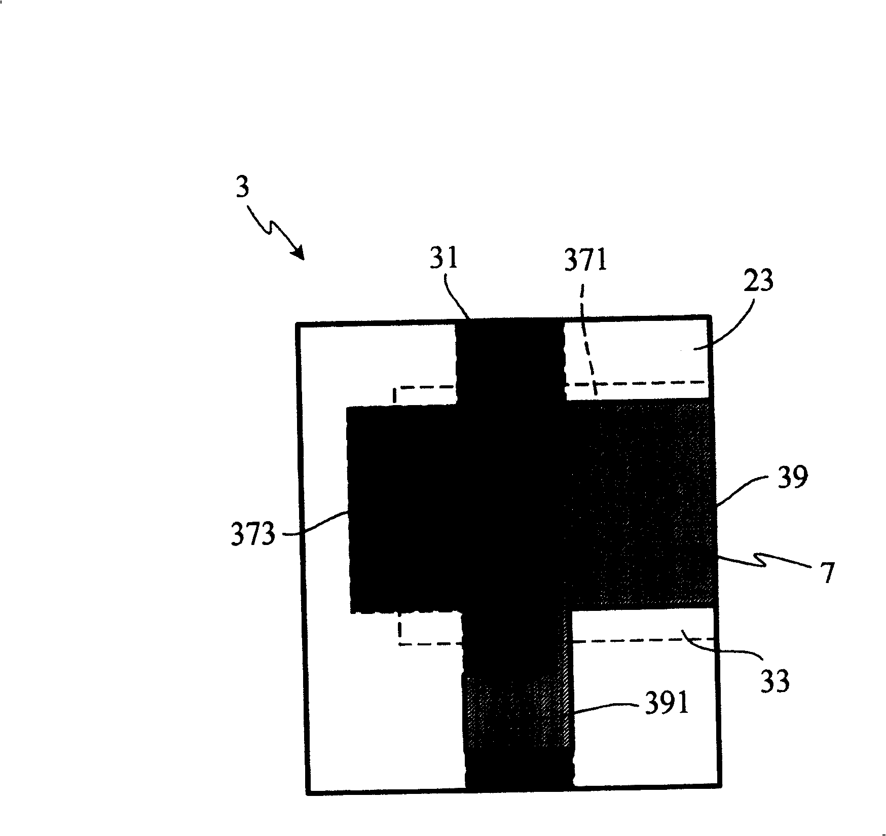
[0043] In detail, the transistor structure 3 sequentially includes a first conductive layer 31 , a dielectric layer 21 , an amorphous silicon layer 33 , an electrode layer 35 , a second conductive layer 37 , a flat dielectric layer 23 and an upper gate 39 . Wherein, the dielectric layer 21 covers the first conductive layer 31, the amorphous silicon layer 33 partially covers the dielectric layer 21, and the electrode layer 35 is arranged on the amo...


PUM


Abstract

The structure of the transistor includes first conductive layer, second conductive layer and upper grid. The structure of the transistor forms fortified capacitance among first conductive layer, second conductive layer and upper grid so as to reduce circuit area possessed by setting up additional capacitance greatly. Or, the invention raises capacity of capacitance without need of setting up additional capacitance.

Description

technical field [0001] The invention relates to a transistor structure and a control unit with the transistor structure; in particular, a transistor structure and a control unit for a liquid crystal display driving circuit. Background technique [0002] Due to the advantages of power saving, light weight, low radiation and easy portability, liquid crystal displays have become mainstream products on the market. For a Thin Film Transistor Liquid Crystal Display (TFT-LCD), it is mainly composed of a display panel and a backlight assembly, wherein the display panel includes a transistor array, a color filter substrate and liquid crystals poured therein. Through the operation of the above components, the function of image display is provided. [0003] Generally speaking, on the external drive circuit of the LCD screen, in addition to transistors, additional large capacitors must be provided to provide a voltage stabilizing effect. However, the large capacitors usually occupy a ...

Claims


Application Information

Patent Timeline
Patent Type & Authority Patents(China)
IPC IPC(8): H01L29/41H01L29/78H01L27/12
Inventor 梁中瑜魏俊卿
Owner AU OPTRONICS CORP
Why Eureka
Try Eureka