High voltage N-shape metal oxide semiconductor tube and its preparing method

A technology of semiconductor tubes and oxides, which is applied in the fields of semiconductor/solid-state device manufacturing, semiconductor devices, electrical components, etc., can solve the problems of insufficient comprehensiveness, without considering the thickness of the oxide layer, field plate, etc., and achieves low manufacturing cost and conduction. The effect of resistance reduction and breakdown voltage improvement

Inactive Publication Date: 2009-03-18
SOUTHEAST UNIV
View PDF1 Cites 2 Cited by
  • Summary
  • Abstract
  • Description
  • Claims
  • Application Information

AI Technical Summary

Problems solved by technology

However, the current linear implantation technology in the drift region is one-dimensional, and does not take into account the influence of different oxide layer thicknesses and field plates, so it is not comprehensive enough.

Method used


Image

  • High voltage N-shape metal oxide semiconductor tube and its preparing method
  • High voltage N-shape metal oxide semiconductor tube and its preparing method
  • High voltage N-shape metal oxide semiconductor tube and its preparing method

Examples


Embodiment 1

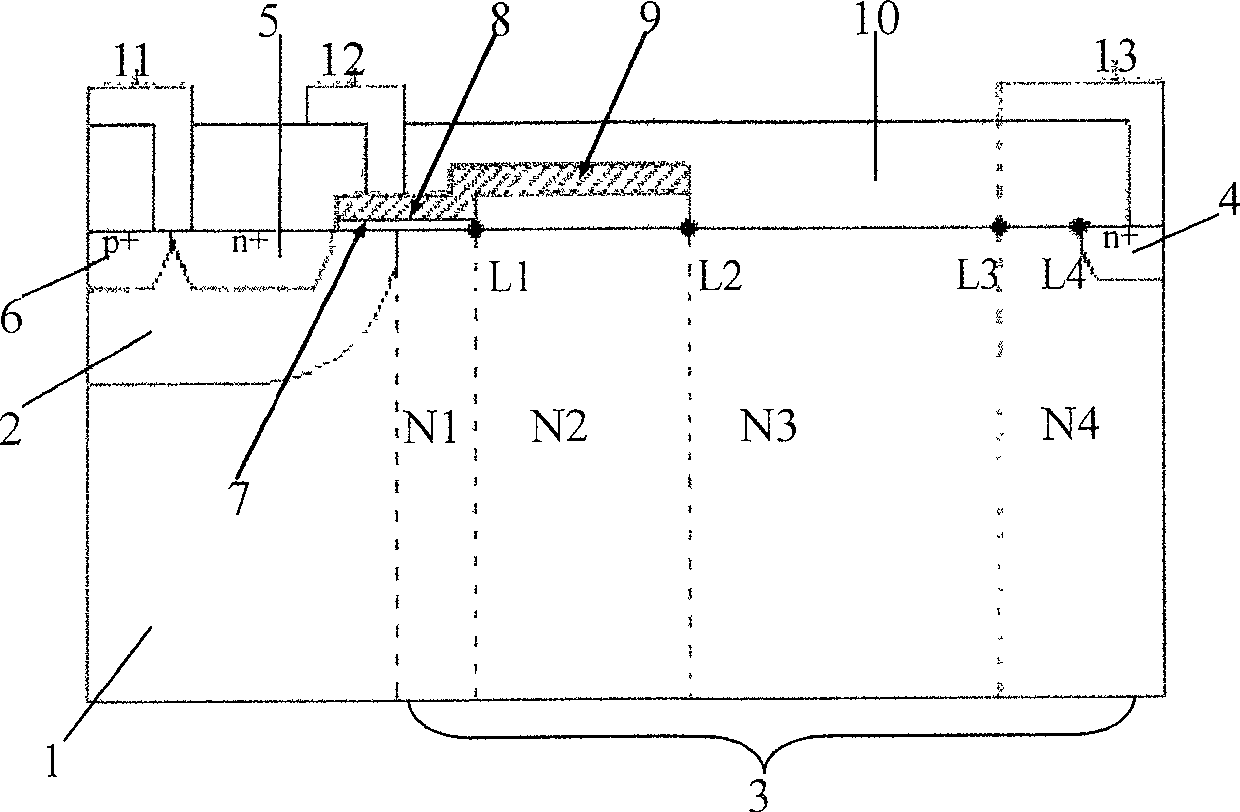
[0015] refer to figure 1 , a linearly doped high-voltage N-type metal oxide semiconductor tube, comprising an N-type substrate 1, a P-type well 2 and an N-type drift region 3 are arranged on the N-type substrate 1, and a P-type well 2 is arranged in the P-type well 2 There are P-type contact hole 6 and N-type source 5, N-type drain 4 is arranged in N-type drift region 3, gate oxide layer 7 is arranged above P-type well 2 and N-type drift region 3, and gate oxide layer 7 is provided with a polysilicon gate 8 and the polysilicon gate 8 is located above the junction of the P-type well 2 and the N-type drift region 3, a field oxide layer 10 is provided above the gate oxide layer 7 and the polysilicon gate 8, and the P-type contact hole 6 An aluminum lead 11 is connected to the N-type source 5, an aluminum lead 12 is connected to the polysilicon gate 8, an aluminum lead 13 is connected to the N-type drain 4, and a polysilicon field plate 9 is arranged in the field oxide layer 10. T...

Embodiment 2

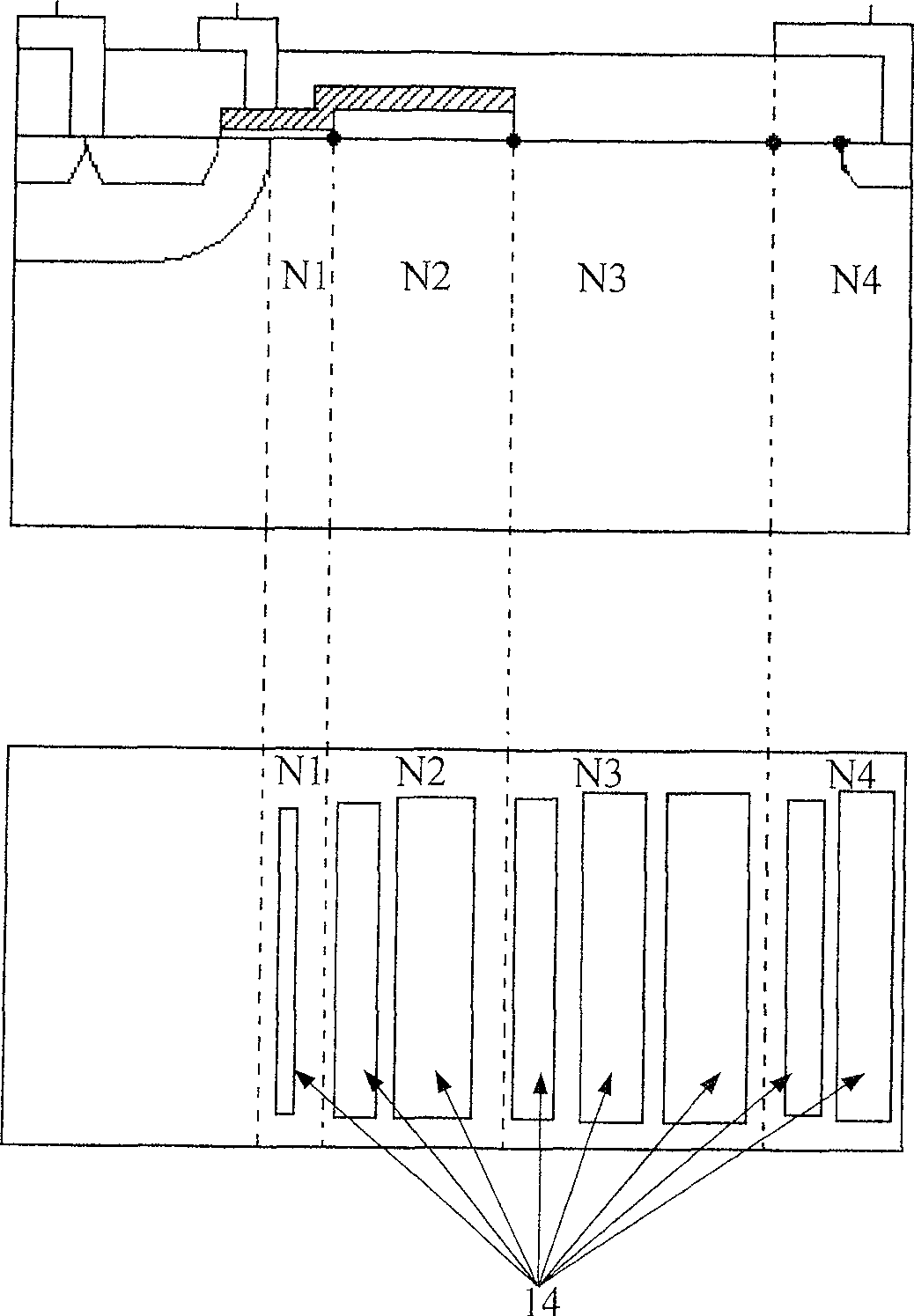
[0017] A preparation method for manufacturing the above-mentioned high-voltage N-type metal oxide semiconductor tube, first prepare an N-type substrate with a concentration of 1×10 15 cm -3 Next, prepare an N-type drift region on the N-type substrate. The drift zone is linearly implanted in four regions, and the implantation windows from small to large are sequentially opened on the photolithography plates of the first to fourth drift regions. After ion implantation, After thermal diffusion, the impurities form a segmented linear distribution in the drift region. After that, the field oxide layer, gate oxide layer, polysilicon gate, P-type well, N-type source, drain and N-type substrate contact holes and contact holes and metal aluminum leads.

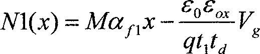
[0018] refer to figure 2 , when the N-type drift region is prepared on the N-type substrate, the drift zone has four linear implants, and each part is doped according to the following equation.

[0019] ...


PUM


Abstract

This invention relates to a high pressure N-type MOS tube with linear dope, in which, a P-type trap and a N-type drift region are set on the N-type substrate, a P-type contact hole and a N-type source are set in the P-type trap, a N-type leak is set in the N-type drift region, a grid oxidation layer is set above the P-type trap and the N-type drift region, a polysilicon grid is set above the grid oxidation layer and above the interface of the trap and the drift region, a filed oxidation layer is set above the grid oxidation layer and the polysilicon grid, Al leads are connected on the contact hole, the N-type sourc, the polysilicon grid and the N-type leak, polysilicon field pole plates connected with the polysilicon grid are set in the field oxidation layer, the N-type drift region is composed of a first, second, third and fourth regions arrayed along the source and the leak orderly, the doped concentration becomes smaller from the fourth, third, second and the first region.

Description

technical field [0001] The invention relates to a metal oxide semiconductor tube and a preparation method thereof, especially a high-voltage N-type metal oxide semiconductor tube and a preparation method thereof. Background technique [0002] Metal oxide semiconductor power devices have the advantages of good switching characteristics and low power consumption. More importantly, metal oxide semiconductor power devices are easily compatible with standard low-voltage metal oxide semiconductor processes and reduce chip production costs. Therefore, in 10V- Within the application range of 600V, metal oxide semiconductor power devices are widely used in power integrated circuits. Breakdown voltage and on-resistance are the two most critical parameters of high-voltage metal oxide semiconductor devices, and they are also a pair of contradictions. As the breakdown voltage increases, the on-resistance increases accordingly. Recently, some new technologies or new structures have emerg...

Claims


Application Information

Patent Timeline
Patent Type & Authority Patents(China)
IPC IPC(8): H01L29/78H01L21/336
Inventor 孙伟锋易扬波李海松陆生礼时龙兴
Owner SOUTHEAST UNIV
Why Eureka
Try Eureka