Field emission display device and method of manufacturing same

A display device and electric field emission technology, applied in the direction of electrode device and related components, electrode system manufacturing, non-luminescent electrode manufacturing, etc., can solve the problem of not being able to densely form openings, difficulty in forming openings, deviation of the total amount of electron beams, etc. question

Inactive Publication Date: 2009-07-29
MITSUBISHI ELECTRIC CORP
View PDF6 Cites 0 Cited by
  • Summary
  • Abstract
  • Description
  • Claims
  • Application Information

AI Technical Summary

Problems solved by technology

[0009] Moreover, if the assembly position of the control electrode is shifted, the size of the overlapping range of the opening range of the corresponding electron passing hole of the control electrode and the opening range of the corresponding opening of the control electrode is different between each phosphor, and the size of the range is different. The total amount of electron beams flowing into each phosphor varies, and the amount of light emitted by each phosphor is uneven, which impairs the uniformity of light emission on the phosphor surface (display surface) of an electric field emission display device.
And such defective products lead to increased manufacturing costs
[0010] Moreover, since the opening that passes through the control electrode and the insulator layer is formed in a circular shape, if the opening diameter of the opening is reduced, it is difficult for the developer to flow to the bottom of the opening when the opening is formed, and the formation of the opening needs more time. time, the formation of openings becomes difficult
For this reason, the opening diameter of the opening had to be increased. As a result, the openings could not be densely formed, and there was a problem that the total amount of electron beams decreased.

Method used


Image

  • Field emission display device and method of manufacturing same
  • Field emission display device and method of manufacturing same
  • Field emission display device and method of manufacturing same

Examples


Embodiment Construction

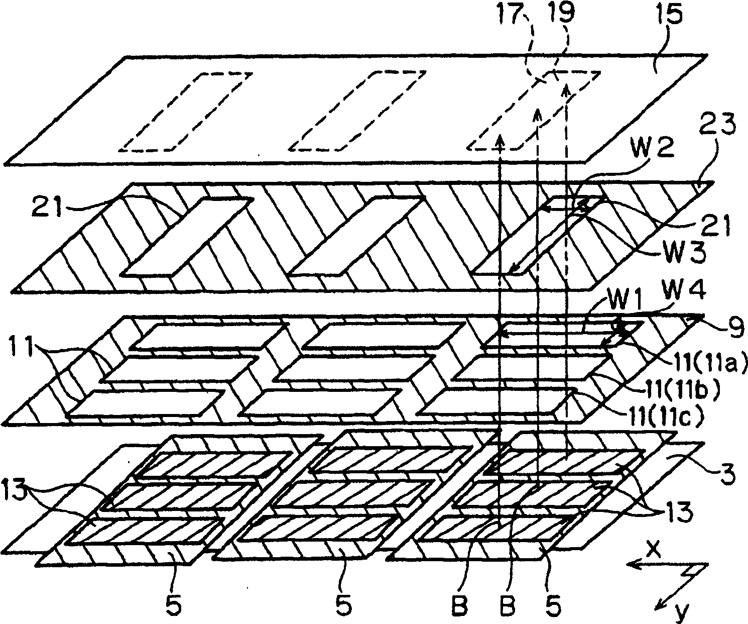
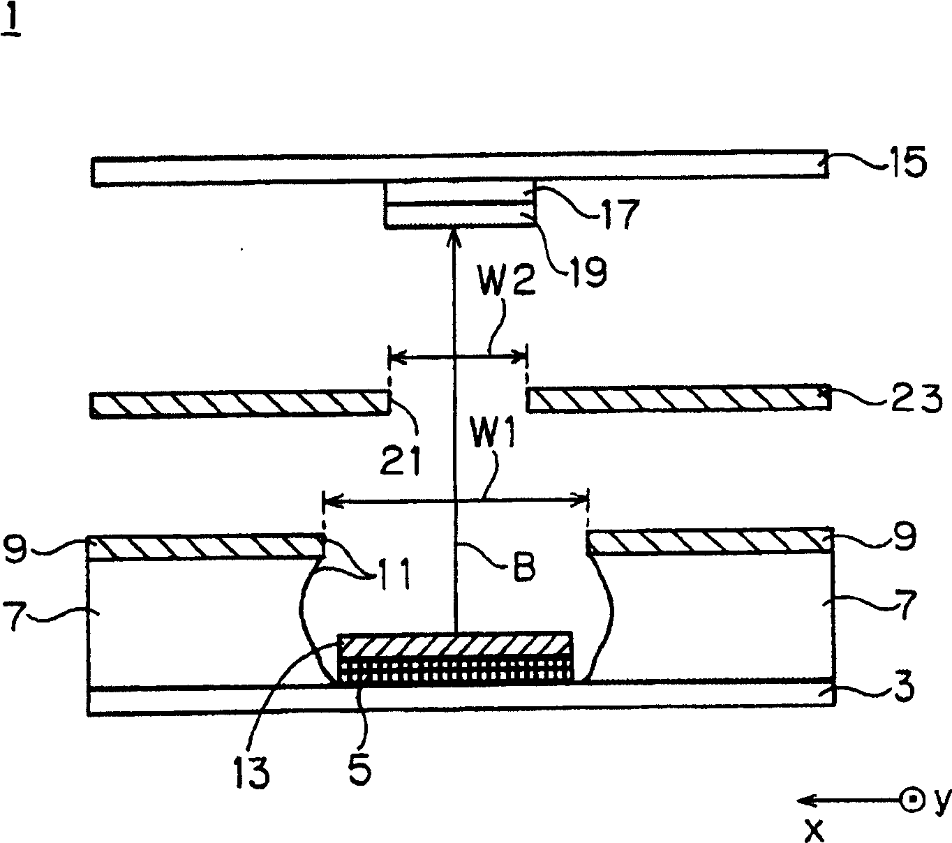
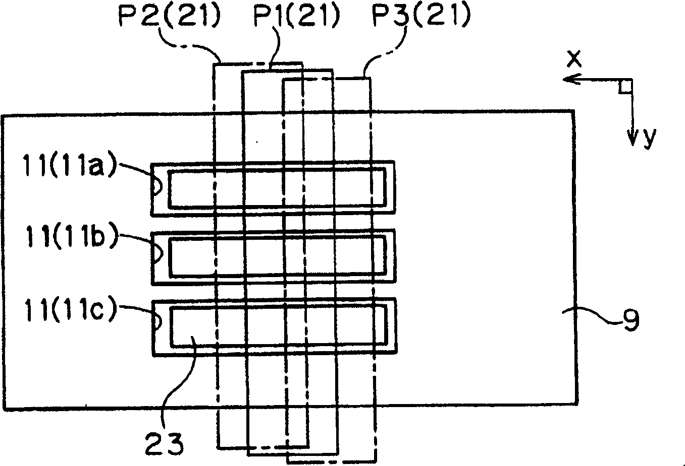
[0022] like figure 1 and figure 2 As shown, the field emission display device 1 of this embodiment includes: a cathode substrate 3; a cathode 5 formed on the cathode substrate 3; The same flat type electron emission material layer 13; the control electrode 9 which is arranged on the front side of the electron emission material layer 13 and has an opening 11 formed on the part opposite to the electron emission material layer 13; A transparent anode substrate 15 arranged in the front; a transparent anode 17 formed on the back side of the anode substrate 15; a phosphor 19 formed on the anode 17; The shielding electrode 23 of the electron passing hole 21 passes the electron beam B flowing from the electron emission material layer 13 into the phosphor 19 through the opening 11 of the control electrode 9 .

[0023] Here, an insulator layer 7 is formed on the cathode substrate 3 and the cathode 5 , and a control electrode 9 is formed on the insulator layer 7 . Opening 11 is form...


PUM


Abstract

Provided are an electric field emission display device and a method of manufacturing the same, capable of assembling a shielding electrode in such a manner that uniformity of light emission on a fluorescent surface (display surface) can be maintained without requiring high assembling accuracy. In this field emission display device (1), the opening width (W1) of the opening (11) of the control electrode (9) in a predetermined direction (x direction) is formed to be larger than the electron passing hole (W1) of the shielding electrode (23). 21) The opening width (W2) in the above-mentioned predetermined direction is large, and the entire range of the opening width (W2) in the above-mentioned predetermined direction of the electron passing hole (21) of the shielding electrode (23) overlaps the opening of the control electrode (9) (11) The shielding electrode (23) is arranged on the front side of the control electrode (9) so as to be within the range of the opening width (W1) in the predetermined direction.

Description

technical field [0001] The present invention relates to an electric field emission display device which improves the uniformity of light emission on a fluorescent surface (display surface) of the electric field emission display device and a method for manufacturing the same. Background technique [0002] Generally, the main structure of an electric field emission display device includes: a cathode substrate formed with a cathode; an insulator layer formed on the above-mentioned cathode substrate and the above-mentioned cathode; a control electrode formed on the above-mentioned insulator layer; An electron emission material layer formed on the cathode in the opening formed by the insulator layer and exposed from the bottom of the opening; and an anode substrate on which an anode and a phosphor are formed in front of the control electrode (Patent Document 1, 2). In such a conventional field emission display device, the opening of the control electrode is formed in a circular ...

Claims


Application Information

Patent Timeline
Patent Type & Authority Patents(China)
IPC IPC(8): H01J31/12H01J9/02H01J1/62H01J9/00H01J9/14H01J9/24H01J29/04H01J29/46H01J29/48H01J63/04
CPCH01J29/467H01J31/127H01J2329/4617H01J2329/4604H01J9/148
Inventor 大野克巳
Owner MITSUBISHI ELECTRIC CORP
Why Eureka
Try Eureka