Method for preparing semi-conductive single-walled carbon nanotubes

A single-walled carbon nanotube, semiconducting technology, which is applied in the field of preparing semiconducting single-walled carbon nanotubes, can solve the problems of complex processing, carbon nanotube damage, difficult application, etc., and achieve simple equipment, original appearance, and low cost Effect

Inactive Publication Date: 2009-12-16
PEKING UNIV
View PDF4 Cites 0 Cited by
  • Summary
  • Abstract
  • Description
  • Claims
  • Application Information

AI Technical Summary

Problems solved by technology

There are some shortcomings in these methods: or, there will be damage to the carbon nanotubes; or, the processing process is complicated, and it is difficult to apply in industry

Method used


Image

  • Method for preparing semi-conductive single-walled carbon nanotubes
  • Method for preparing semi-conductive single-walled carbon nanotubes
  • Method for preparing semi-conductive single-walled carbon nanotubes

Examples


Embodiment 1

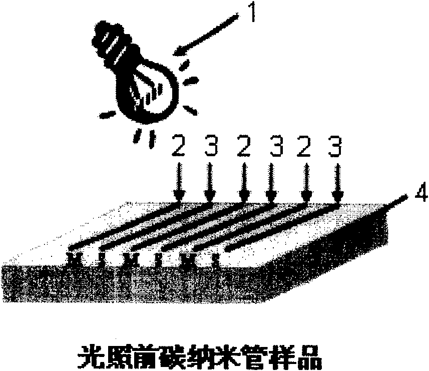
[0020] (1) A high-density array of single-walled carbon nanotubes oriented along the sapphire [1-100] lattice direction is grown on the surface of an A-plane sapphire single crystal by chemical vapor deposition (CVD). See attached figure 2 (a).

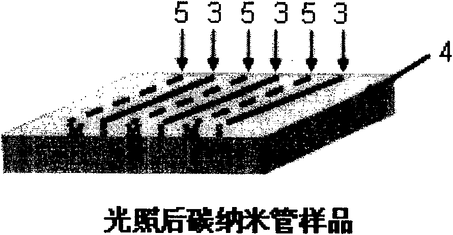
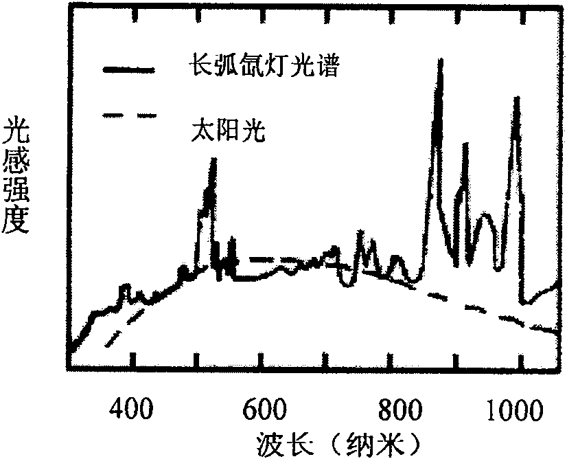
[0021] (2) Use a long-arc xenon lamp to illuminate the single-walled carbon nanotube array sample, and keep the surface light intensity of the single-walled carbon nanotube sample at 75mW / cm 2 , in the air for 60 minutes. See attached figure 2 (b).

[0022] (3) For 39 points in the same region on the same sample, corresponding to different illumination times (0min, 30min, 60min), respectively use Raman spectra with laser wavelengths of 633nm and 514nm for characterization. See attached figure 2 (c), attached figure 2 (d).

[0023] attached by figure 2 It can be seen that after 30 minutes of light irradiation, the Raman signal (M) of metallic single-walled carbon nanotubes in the single-walled carbon nanotube array decreas...

Embodiment 2

[0025] (1) Using chemical vapor deposition (CVD) to grow high-density single-walled carbon nanotubes on a silica substrate. See attached image 3 (a).

[0026] (2) Use a long-arc xenon lamp to illuminate the single-walled carbon nanotubes, and keep the surface light intensity of the single-walled carbon nanotubes at 75mW / cm 2 , lighted in the air for 30min. See attached image 3 (b).

[0027] (3) For 39 points in the same area on the same sample, corresponding to different illumination times (0min, 30min, 60min), use the Raman spectrum with a laser wavelength of 633nm to characterize, and use the Raman spectrum with a laser wavelength of 514nm to illuminate The samples after 60 min were characterized. See attached image 3 (c).

[0028] attached by image 3It can be seen that after 30 min of light irradiation, the Raman signal (M) of metallic single-wall carbon nanotubes in single-wall carbon nanotubes decreases sharply; after 60 min of light irradiation, in the single...

Embodiment 3

[0030] (1) Using chemical vapor deposition (CVD) to grow high-density single-walled carbon nanotube arrays on the A-plane sapphire single crystal substrate, and transfer the single-walled carbon nanotube arrays to the carbon dioxide on a silicon substrate. See attached Figure 4 (a).

[0031] (2) Use a long-arc xenon lamp to illuminate the single-walled carbon nanotube array sample, and keep the surface light intensity of the single-walled carbon nanotube sample at 75mW / cm 2 , in the air for 120min.

[0032] (3) The samples after irradiating for 120 min were characterized by Raman spectrum with a laser wavelength of 633 nm. See attached Figure 4 (b).

[0033] attached by Figure 4 It can be seen that after 120min of light irradiation, the Raman signal (M) of the metallic single-walled carbon nanotubes is very little (160cm -1 -230cm -1 ), mainly the Raman signal (S) of semiconducting single-walled carbon nanotubes (-1 area). It can be seen that after 120 minutes of l...


PUM

PropertyMeasurementUnit
strengthaaaaaaaaaa

Abstract

The invention discloses a method of preparing semi-conductor single-wall carbon nanometer tube by removing the metallic single-wall carbon nanometer tube in the single-wall carbon nanometer tube, the single-wall carbon nanometer tube is irradiated under a certain strength light so as to remove the metallic single-wall carbon nanometer tube, thereby obtaining the semi-conductor single-wall carbon nanometer tube, wherein total strength of the light that is irradiated on the surface of the carbon nanometer tube sample and has wave length range of 180nm-11um is 30mW per square centimeter to 300mW per square centimeter, compared with the prior art, the invention has the advantages of simple and controllable operation, environmental protection, good effect for removing metallic single-wall carbon nanometer tube, wide adaptability, low cost, and keeping the original look of carbon tube. The utility model has strong practicality and wide application prospect.

Description

technical field [0001] The invention relates to a method for preparing semiconducting single-wall carbon nanotubes. Background technique [0002] Carbon nanotubes have excellent electrical and mechanical properties and are ideal one-dimensional nanomaterials. Among them, metallic single-walled carbon nanotubes are ideal one-dimensional wires, while semiconducting single-walled carbon nanotubes can be used to build various electronic devices at the nanometer scale, and are expected to replace silicon materials in the future to build next-generation devices. [0003] At present, the methods for preparing single-walled carbon nanotubes mainly include laser ablation, arc discharge and chemical vapor deposition (CVD). Among them, the carbon nanotubes synthesized by the chemical vapor deposition method are relatively pure and can be directly used to construct carbon nanotube devices. However, the single-walled carbon nanotubes synthesized by these preparation methods are all mix...

Claims


Application Information

Patent Timeline
Patent Type & Authority Patents(China)
IPC IPC(8): C01B31/02B82B3/00
CPCY10S977/845C01B2202/02B82Y30/00C01B2202/22C01B31/0266B82Y40/00B82B3/00Y10S977/734C01B31/0293C01B32/172C01B32/18
Inventor 张锦张永毅张依刘忠范
Owner PEKING UNIV
Why Eureka
Try Eureka