Metastable state assistant quantum dot resonance tunneling diode and working condition

A technology of resonant tunneling and quantum dots, applied in diodes and other directions, can solve problems such as limiting the wide application of single-electron devices, and achieve the effects of expanding applications, simple diode structure, and increasing operating temperature.

Inactive Publication Date: 2010-01-13
SHANGHAI INST OF TECHNICAL PHYSICS - CHINESE ACAD OF SCI
View PDF4 Cites 22 Cited by
  • Summary
  • Abstract
  • Description
  • Claims
  • Application Information

AI Technical Summary

Problems solved by technology

When the temperature-induced thermal fluctuation is close to the sum of Coulomb energy and sub-level spacing (also known as charge injection energy), the single-electron tunneling feature is affected by thermal disturbance (or called thermal smear effect) no longer exists; The thermal fluctuation (KT 300K ~25.9meV) charge injection energy, its spatial scale must be about 10 nanometers or even smaller in three dimensions, which puts forward extremely high requirements for semiconductor process technology; therefore, the current main semiconductor single-electron tunneling devices are all Can only work at low temperature, which limits the wide application of single-electron devices

Method used


Image

  • Metastable state assistant quantum dot resonance tunneling diode and working condition
  • Metastable state assistant quantum dot resonance tunneling diode and working condition
  • Metastable state assistant quantum dot resonance tunneling diode and working condition

Examples


Embodiment Construction

[0039] Below by embodiment, the specific embodiment of the present invention is described in further detail:

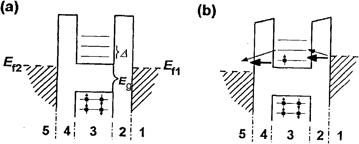
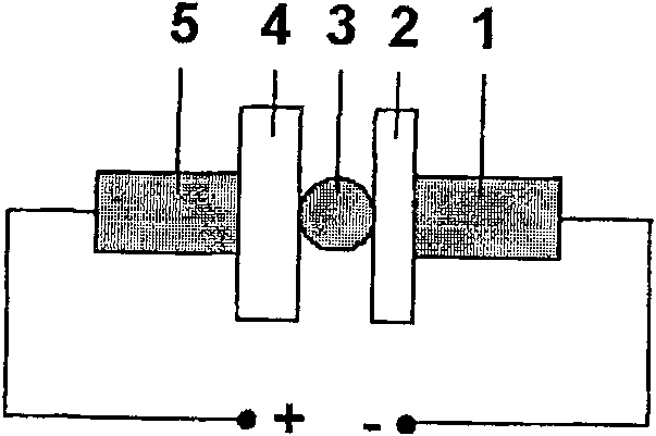
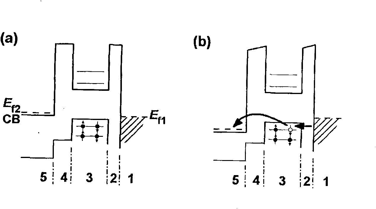
[0040]The embodiment provides a prototype structure of an InAs / GaAs surface quantum dot double barrier diode working at room temperature and a preparation method thereof. In this method, an n-type GaAs collector layer 5 is first formed on a GaAs substrate 6 and then an intrinsic GaAs second tunneling layer 4 is formed on the collector layer. Thereafter, an InAs quantum dot layer 3 is formed on the GaAs second tunneling layer. Then, an oxidized first tunneling layer 2 is formed on the surface of the InAs quantum dots. Finally, a conductive scanning probe is used as the metal emitter 1 .

[0041] The thickness of the n-type GaAs collector layer is 1000 nm, and the doping concentration of n-type Si is 1×10 18 cm -3 ;

[0042] The thickness of the intrinsic GaAs second tunneling layer is less than 4 atomic layers;

[0043] The base diameter of the InAs quantum dot s...


PUM


Abstract

The invention provides a semiconductor quantum-dot metastable resonant tunneling diode structure and the working conditions. The structure includes: a substrate and a growth collector, a second tunnel barrier layer, quantum dots which are coupled between an emitter and the collector, a first tunnel barrier layer and the emitter which are sequentially arranged on the substrate. The working conditions include working temperature, working bias voltage and the obtainment of the metastable state of the quantum dots. The invention can eliminate the impact of the neighboring sub-level of the quantum dots on the metastable single-electron tunneling so as to achieve the purpose of improving the working temperature of the diode.

Description

technical field [0001] The invention relates to a semiconductor single-electron device, in particular to a diode structure design and working conditions for realizing single-electron resonant tunneling by utilizing quantum dot metastable state. Background technique [0002] Semiconductor double-barrier resonant tunneling diode (DB-RTD) is an electronic device that uses bound energy states to realize quantum tunneling transport; Discrete energy states can only accommodate one electron at the same time, so the resonant tunneling process of electrons through these atomic-like energy level systems becomes a single-electron tunneling process.Single-electron tunneling constitutes a limit case for electronic devices, which at the level of a single energy state Realize the control of the current, so it has important applications in some current cutting-edge technology fields, such as highly sensitive potentiometers, high quantum efficiency photodetectors, etc., and is also a possibl...

Claims


Application Information

Patent Timeline
Patent Type & Authority Patents(China)
IPC IPC(8): H01L29/88
Inventor 陆卫李天信陈平平张波甄红楼李志锋李宁陈效双
Owner SHANGHAI INST OF TECHNICAL PHYSICS - CHINESE ACAD OF SCI
Why Eureka
Try Eureka