
Semiconductor device and manufacturing method thereof

A manufacturing method and semiconductor technology, applied in semiconductor/solid-state device manufacturing, semiconductor devices, transistors, etc., can solve the problem that the size of NPN transistor 61 equipment is difficult to reduce, and achieve the effect of reducing crystal defects and reducing the size of equipment

Inactive Publication Date: 2010-01-27
SANYO ELECTRIC CO LTD
View PDF4 Cites 0 Cited by
  • Summary
  • Abstract
  • Description
  • Claims
  • Application Information

AI Technical Summary

Problems solved by technology

Therefore, since the lateral diffusion widths W4, W5 of the P-type buried diffusion layers 64, 65 become wider, there is a problem that it is difficult to reduce the device size of the NPN transistor 61.

Method used


Image

  • Semiconductor device and manufacturing method thereof
  • Semiconductor device and manufacturing method thereof
  • Semiconductor device and manufacturing method thereof

Examples


Embodiment Construction

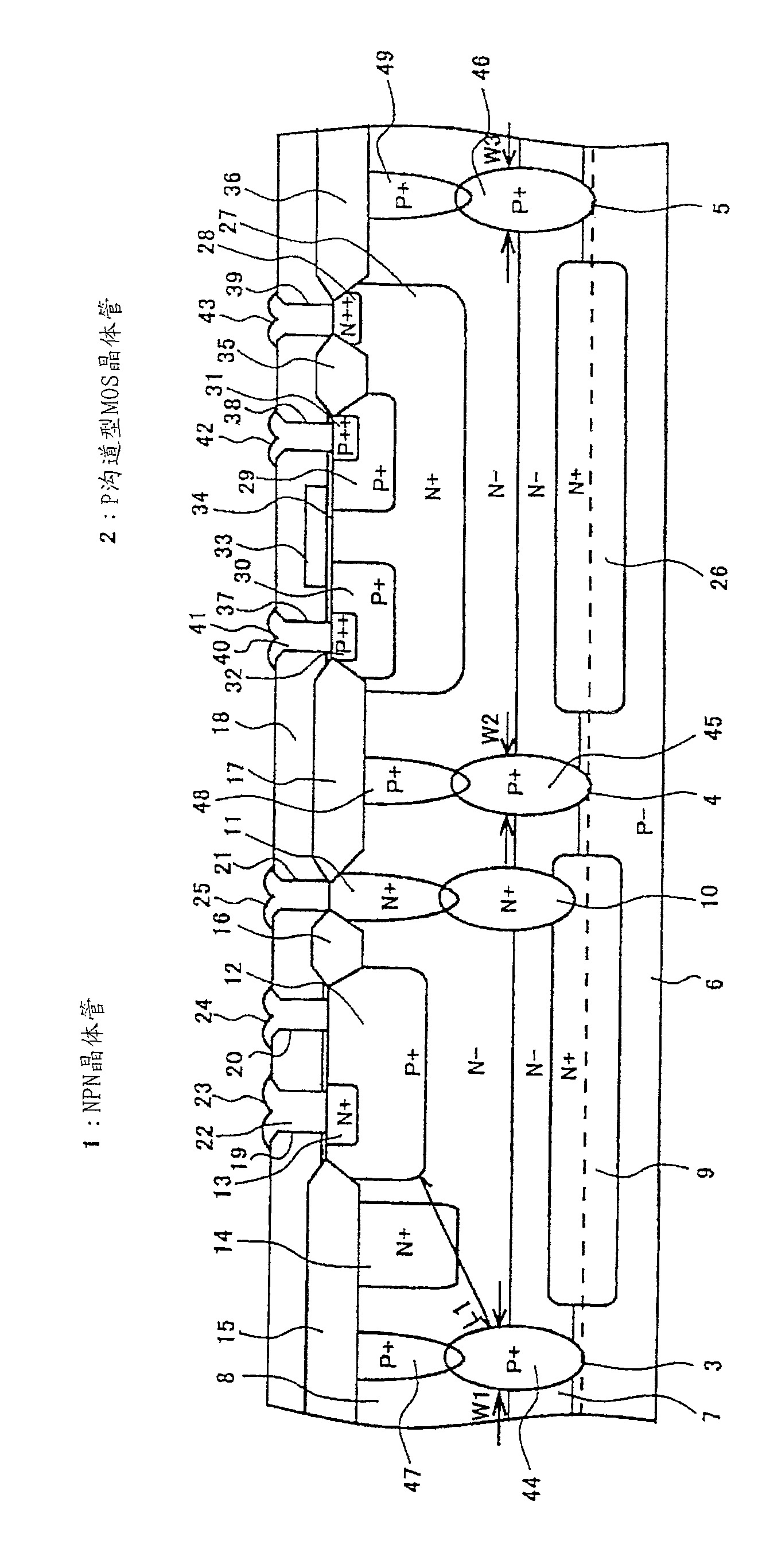
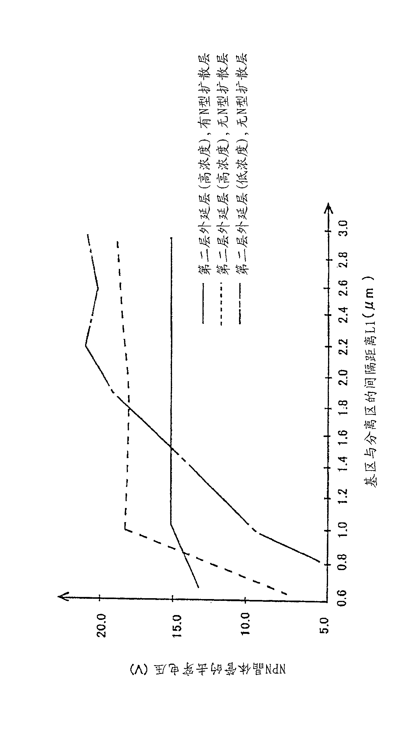
[0040] Below, refer to Figure 1 ~ Figure 2 The semiconductor device according to the embodiment of the present invention will be described in detail. figure 1 is a cross-sectional view illustrating a semiconductor device according to an embodiment of the present invention, figure 2 It is a graph for explaining the withstand voltage characteristic of the semiconductor device according to the embodiment of the present invention.

[0041] Such as figure 1 As shown, an NPN transistor 1 is formed in one element formation region divided by isolation regions 3 , 4 , and 5 , and a P-channel MOS (Metal Oxide Semiconductor) transistor 2 is formed in another element formation region. In addition, although not shown, N-channel MOS transistors, PNP transistors, and the like are formed on other element formation regions.

[0042] As shown in the figure, the NPN transistor 1 is mainly composed of a P-type monocrystalline silicon substrate 6, N-type epitaxial layers 7, 8, N-type buried...


PUM


Abstract

The invention provides a semiconductor device and a manufacturing method thereof. In a conventional semiconductor device, because the horizontal diffuse width of a P type embedding diffuse layer which constitutes a separating region become wider, desired anti-pressing characteristic is difficult to be obtained. In a semiconductor device of the present invention, two epitaxial layers are formed on a P type single crystal silicon substrate. One of the epitaxial layers has an impurity concentration higher than that of the other epitaxial layer. The epitaxial layers are divided into a plurality of element formation regions by isolation regions. In one of the element formation regions, an NPN transistor is formed. Moreover, between a P type diffusion layer, which is used as a base region of the NPN transistor, and a P type isolation region, an N type diffusion layer is formed. Use of this structure makes it hard for a short-circuit to occur between the base region and the isolation region. Thus, the breakdown voltage characteristics of the NPN transistor can be improved.

Description

technical field [0001] The present invention relates to a semiconductor device that maintains withstand voltage characteristics and reduces the size of the device and its manufacturing method. Background technique [0002] As an example of a conventional semiconductor device, the structure of the NPN transistor 61 described below is well known. Such as Figure 9 As shown, an N-type epitaxial layer 63 is formed on a P-type semiconductor substrate 62 . On the epitaxial layer 63 are formed P-type buried diffusion layers 64 and 65 diffused upward and downward (depth direction) from the surface of the substrate 62 and P-type diffused layers 66 and 67 diffused from the surface of the epitaxial layer 63 . Further, the epitaxial layer 63 is divided into a plurality of element formation regions by the isolation regions 68 and 69 formed by connecting the P-type buried diffusion layers 64 and 65 to the P-type diffusion layers 66 and 67 . On one element forming region, for example, an...

Claims


Application Information

Patent Timeline
Patent Type & Authority Patents(China)
IPC IPC(8): H01L27/06H01L29/73H01L21/822H01L21/331
CPCH01L29/66272H01L29/7833H01L29/7322H01L29/1004H01L27/0623H01L21/8249H01L29/0821H01L21/761H01L21/34H01L21/20
Inventor 相马充畑博嗣赤石实
Owner SANYO ELECTRIC CO LTD
Learn More