High-speed semiconductor waveguide phase-shifter

A phase shifter, semiconductor technology, applied in the direction of instruments, nonlinear optics, optics, etc., can solve the problems of static power consumption, low phase change, and inability to separate polarization, etc., and achieve the effect of cost saving and low optical loss

Active Publication Date: 2007-07-25
LUCENT TECH INC
View PDF0 Cites 8 Cited by
  • Summary
  • Abstract
  • Description
  • Claims
  • Application Information

AI Technical Summary

Problems solved by technology

Lithium niobate (LiNbO 3 ) modulators can be fast and have reasonable voltage requirements, however, they cannot be polarized individually and are not suitable for integration of drive electronics and optics
Integrated doped silica waveguides, also known as silicon optical bench components, offer polarization independence and high integration, however, their maximum switching speed is only in the 1MHz range
Semiconductor modulators (InP or GaAs) can have 40GHz bandwidth; however, polarization independence and mass integrati

Method used


Image

  • High-speed semiconductor waveguide phase-shifter
  • High-speed semiconductor waveguide phase-shifter
  • High-speed semiconductor waveguide phase-shifter

Examples


Embodiment Construction

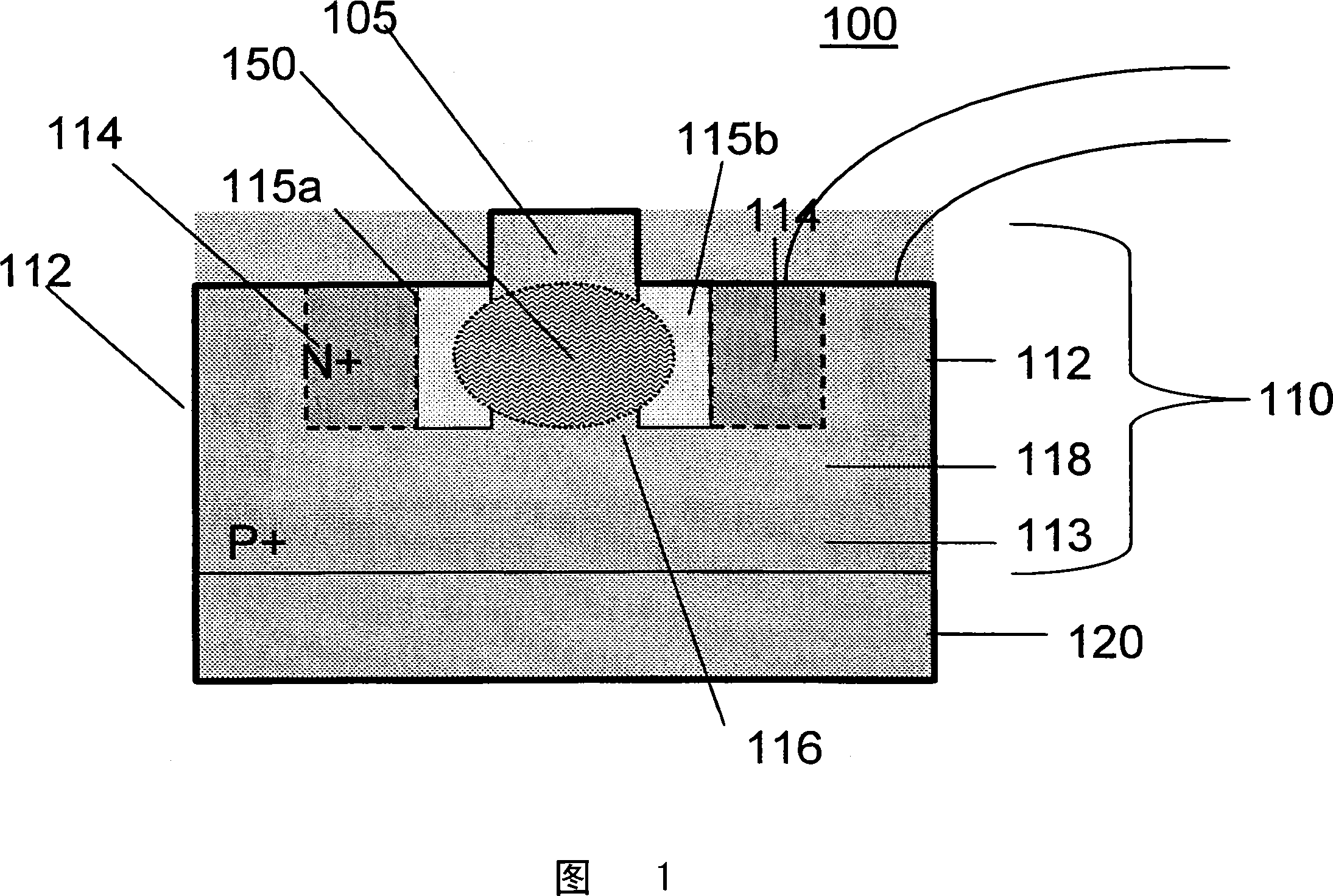
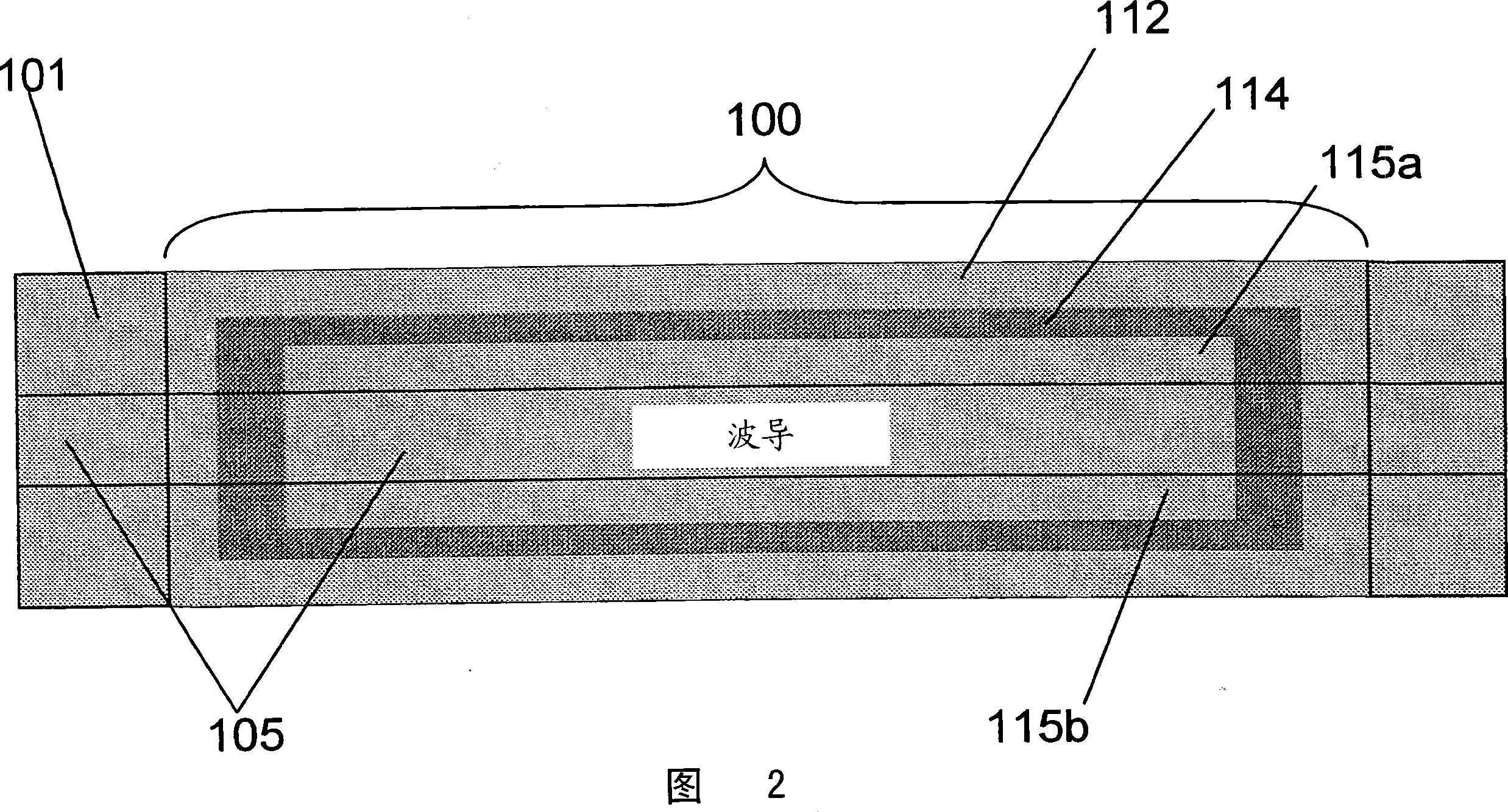
[0016] An exemplary embodiment of the phase shifting device 100 according to the present invention is shown in the cross section of FIG. 1 and in the plan view of FIG. 2. The exemplary device shown is in silica (SiO 2 ) Uses a silicon rib waveguide 110 on the buffer layer 120. The rib 105 is formed on the upper surface of the silicon rib waveguide 110.

[0017] As shown in FIGS. 1 and 2, the silicon rib waveguide 110 has a P-type heavily doped outer region 112 and a base region 113 surrounding the N-type heavily doped inner region 114. The P-type heavily doped outer region 112 extends down to the P-type heavily doped base region 113, and the N-type heavily doped inner region 114 partially extends down to the silicon waveguide 110. Areas 112 and 114 are provided with contacts to allow voltage to be applied across them, as described in more detail below. To prevent leakage current, instead of making direct contact with each other, the heavily doped regions 112 and 114 are preferably...


PUM


Abstract

An optical phase shifter (100) comprises a semiconductor waveguide (105) includes a core region (116) and a doped region (115a, 115b) containing free charges (electrons or holes), which can be steered into or removed from the wave guide, where an optical beam (150) propagates. A semiconductor structure (PN junction 112, 114) allows the control of the amount of free charges in the doped region, which constitutes a potential well. When the well is filled, the charges speed the beam propagation, introducing a phase change. When the well is emptied, (under application of a reverse bias to the junction 112, 114), the beam propagates with extra delay. The phase shifter allows very high speed modulation of the beam using low voltage and low power electronics. The device can be created using standard silicon processing techniques, and integrated with other optical components such as splitters and combiners to create amplitude modulators, attenuators and other optical devices.

Description

[0001] Cross references to related applications [0002] This application is based on and claims the priority of the following applications: U.S. Provisional Patent Application No. 60 / 601,723, which was filed on August 16, 2004 and incorporated herein by reference in its entirety; and U.S. Patent Application No. 11 / 161,744, which was submitted on August 15, 2005 and its entire contents are incorporated herein for reference. Technical field [0003] The present invention relates to the field of high-speed optical communication, and in particular, to a phase shifter device that can change the phase of an optical signal according to an electrical signal. Background technique [0004] The intensity of the light beam is often modulated to encode data in optical communications. This amplitude modulation can be achieved by combining the replication of the selectively delayed beam with itself. When the copy of the beam is delayed by π radians and combined with the original beam, destructi...

Claims


Application Information

Patent Timeline
IPC IPC(8): G02F1/025
Inventor D·M·吉尔C·K·马森C·S·拉费蒂
Owner LUCENT TECH INC
Why Eureka
Try Eureka