Photoelectron characteristic detecting method for thin-layer microcrystal medium material and device thereof

A technology of dielectric materials and detection methods, applied in the direction of measurement devices, analytical materials, material excitation analysis, etc., can solve the problem of inability to distinguish different photogenerated carriers - free and shallow bound photoelectrons, unable to capture photogenerated carrier time signals, etc. question

Inactive Publication Date: 2007-08-15
HEBEI UNIVERSITY
View PDF0 Cites 10 Cited by
  • Summary
  • Abstract
  • Description
  • Claims
  • Application Information

AI Technical Summary

Problems solved by technology

The non-contact method can be used to measure the transient behavior of photogenerated carriers in thin-layer dielectric materials in dispersed systems, but the current existing technology is still not enough to study photosensitivity and luminescence in terms of measurement sensitivity and time resolution. The requirements of the material carrier behavior cannot capture the time signal of the rapid change of photo-generated carriers (ns level), especially the behavior of different photo-generated carriers-free and shallow bound photoelectrons cannot be distinguished, and th

Method used


Image

  • Photoelectron characteristic detecting method for thin-layer microcrystal medium material and device thereof
  • Photoelectron characteristic detecting method for thin-layer microcrystal medium material and device thereof
  • Photoelectron characteristic detecting method for thin-layer microcrystal medium material and device thereof

Examples


Embodiment Construction

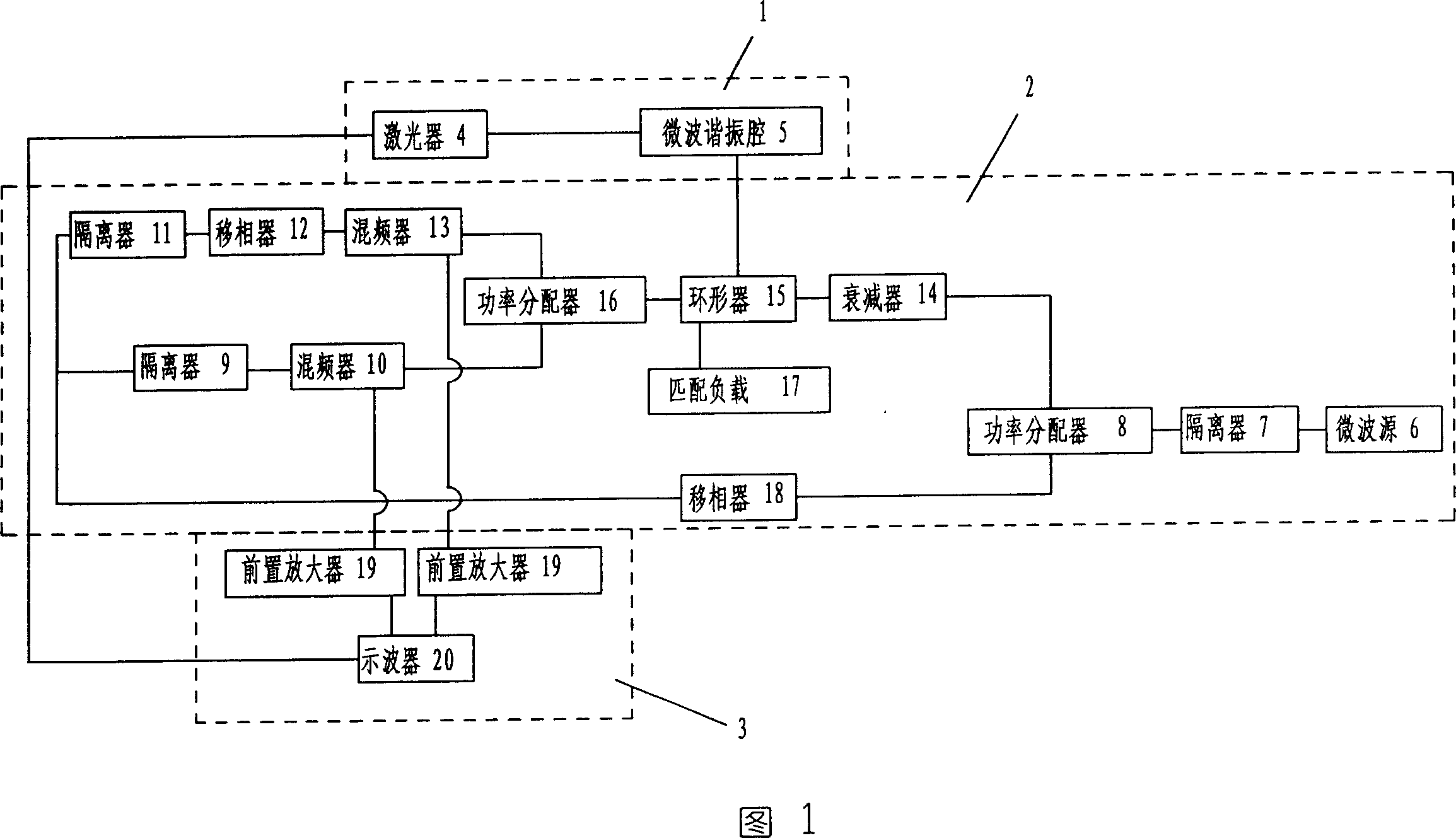
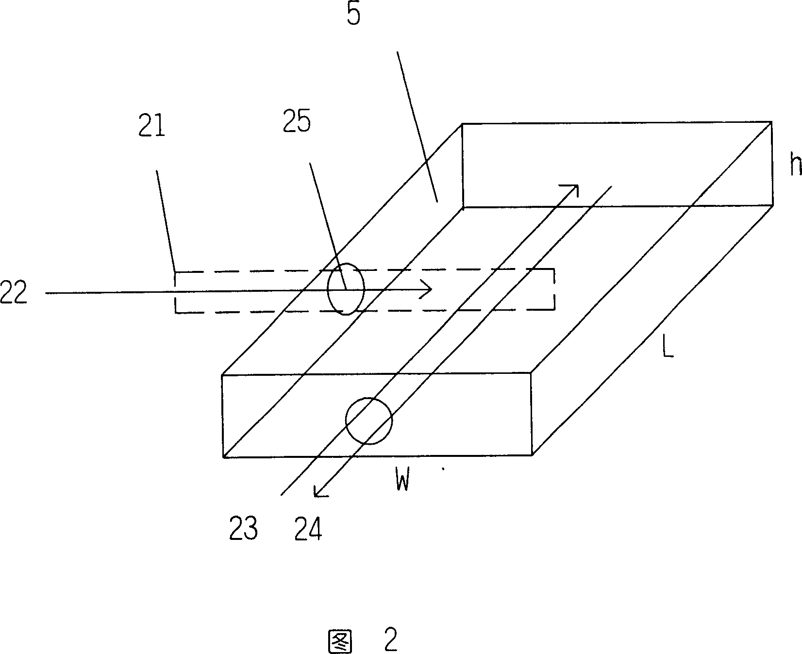
[0026] The method for detecting optoelectronic properties of microcrystalline dielectric thin-layer materials includes an ultrashort pulse laser irradiation part 1 , a microwave phase-sensitive detection part 2 and a data acquisition and processing part 3 . The laser irradiation part 1 generates ultrashort pulse (35ps) laser 22, which is irradiated on the sample 21 standing sideways in the microwave resonator 5 through the light inlet 25, causing the dielectric function of the thin layer material (ε=ε′+iε″ ), the change of the real part ε' and the imaginary part ε" of the material dielectric function changes the properties of the microwave in the microwave resonator. The change of the imaginary part of the dielectric function leads to the absorption of the microwave field in the microwave resonant air by the thin layer dielectric material, and the absorbed microwave power is:

[0027] ΔP=ΔV·E 2 σ=ΔV·eμE 2 no 自由

[0028]where E is the microwave field strength, ΔV is the sam...


PUM

PropertyMeasurementUnit
High haaaaaaaaaa

Abstract

This invention relates to one film transistor medium material photo electron property test method and device, which comprises the following scheme: micro source giving out two paths of micro wave with one for reference signal and other for detection signals into microwave vibration chamber; using laser to light microwave resonance chamber dielectric materials; reflecting detection signals from the chamber into two balance frequency mixture devices; the device makes use of the mixture of the signals by use of phase sensitive technique to isolate micro wave absorptive signals and diffusion signals converted into voltage change; outputting voltage change into computer to get freedom and beam signal range attuning curve.

Description

technical field [0001] The invention relates to a detection method of a dielectric material and a device for realizing the method, which belong to the technical field of measurement. Background technique [0002] The microcrystals in silver halide photosensitive thin-layer materials and zinc sulfide and zinc oxide light-emitting medium thin-layer materials of interest in general applications all have a semiconductor structure. After being excited by light, the photoelectrons in the crystal valence band transition to the conduction band for near-free motion. In the process of movement, it may combine with the traps on the material crystal surface to record optical information, or release a certain amount of energy to relax into the energy storage level in the forbidden band of the crystal, and then return to the valence band in the form of optical radiation after a period of time. Achieve afterglow glow. The movement law of photogenerated carriers is the main factor determin...

Claims


Application Information

Patent Timeline
IPC IPC(8): G01N23/227G01N21/63
Inventor 李晓苇赖伟东杨少鹏张连水傅广生
Owner HEBEI UNIVERSITY
Why Eureka
Try Eureka