Lower voltage conductor-spanning amplifier capable of improving the linearity and input range
A technology of transconductance amplifier and input amplitude, applied in the field of microelectronics and solid-state electronics, can solve the problem of limiting the input amplitude of the source-level attenuation structure, and achieve the effect of low and low resistance node and low level shift
- Summary
- Abstract
- Description
- Claims
- Application Information
AI Technical Summary
Problems solved by technology
Method used
Image
Examples
Embodiment Construction
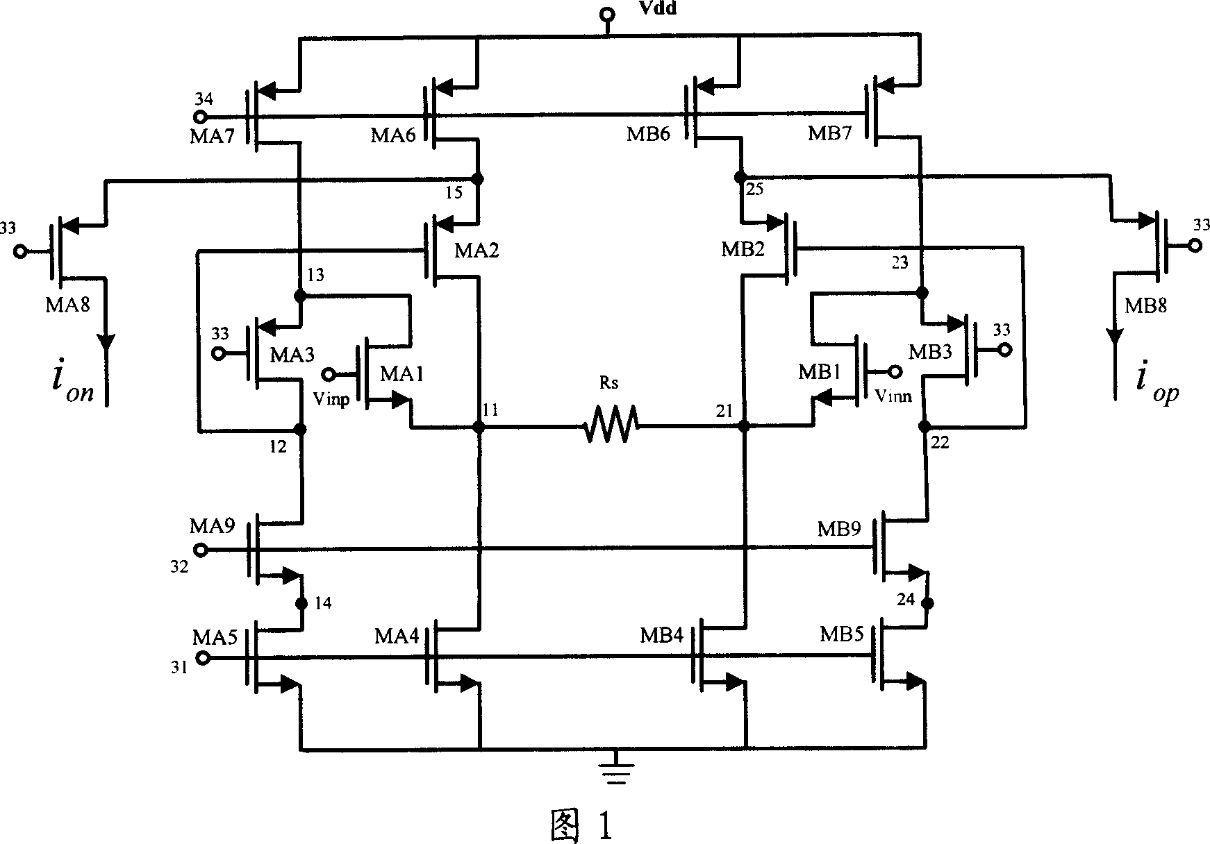
[0022] Technical solution of the present invention refers to Fig. 1. Figure 1 is a low voltage and can improve the linearity and input amplitude transconductance amplifier circuit structure diagram. The source attenuation resistor is R S , MOS tubes (MA1, MA2, MA3, MA5, MA7, MA9, MB1, MA2, MA3, MA5, MA7, MA9) constitute two buffer amplifiers. The current source consists of two P-type MOS tubes (MA6, MB6). The current sink consists of two N-type MOS transistors (MA4, MB4).
[0023] The specific connection relationship of the transconductance amplifier circuit with low voltage and can improve linearity and input amplitude is: two N-type MOS transistors MA1, MB1 constitute two input transistors, in which the gate of MA1 transistor is connected to the positive input terminal of the signal, The drain is connected to node 13, and the source is connected to the source attenuation resistor R through node 11. S , the gate of the MB1 tube is connected to the negative input terminal ...
PUM
 Abstract
Description
Claims
Application Information


